


October 1987
Revised January 1999
MM74C922 • MM74C923
16-Key Encoder • 20-Key Encoder
General Description
The MM74C922 and MM74C923 CMOS key encoders provide all the necessary logic to fully encode an array of SPST switches. The keyboard scan can be implemented by either an external clock or external capacitor. These encoders also have on-chip pull-up devices which permit switches with up to 50 kΩ on resistance to be used. No diodes in the switch array are needed to eliminate ghost switches. The internal debounce circuit needs only a single external capacitor and can be defeated by omitting the capacitor. A Data Available output goes to a high level when a valid keyboard entry has been made. The Data Available output returns to a low level when the entered key is released, even if another key is depressed. The Data Available will return high to indicate acceptance of the new key after a normal debounce period; this two-key roll-over is provided between any two switches.
An internal register remembers the last key pressed even after the key is released. The 3-STATE outputs provide for easy expansion and bus operation and are LPTTL compatible.
Features
■50 kΩ maximum switch on resistance
■On or off chip clock
■On-chip row pull-up devices
■2 key roll-over
■Keybounce elimination with single capacitor
■Last key register at outputs
■3-STATE output LPTTL compatible
■Wide supply range: 3V to 15V
■Low power consumption
Ordering Code:
Order Number |
Package Number |
Package Description |
|
|
|
MM74C922N |
N18A |
18-Lead Plastic Dual-In-Line Package (PDIP), JEDEC MS-001, 0.300” Wide |
|
|
|
MM74C922WM |
M20B |
20-Lead Small Outline Integrated Circuit (SOIC), JEDEC MS-013, 0.300” Wide |
|
|
|
MM74C923WM |
M20B |
20-Lead Small Outline Integrated Circuit (SOIC), JEDEC MS-013, 0.300” Wide |
|
|
|
MM74C923N |
N20A |
20-Lead Plastic Dual-In-Line Package (PDIP), JEDEC MS-001, 0.300” Wide |
|
|
|
Device also available in Tape and Reel. Specify by appending suffix letter “X” to the ordering code.
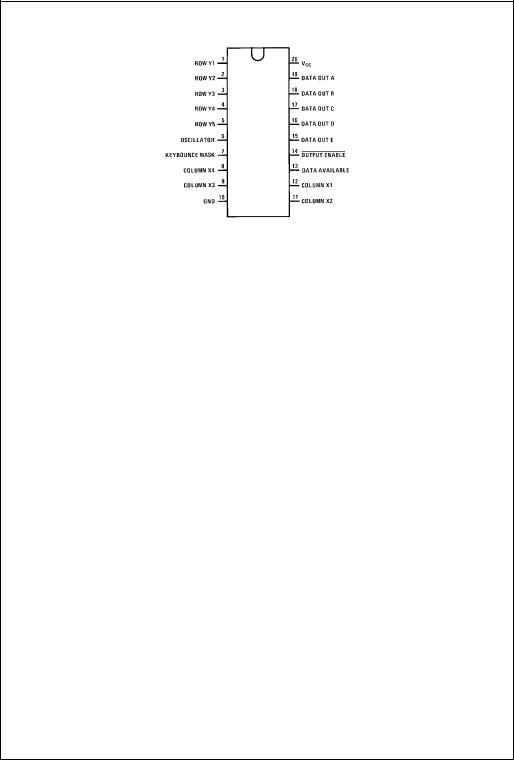
Connection Diagrams
Pin Assignment for DIP Pin Assignment for SOIC
Top View
MM74C922
Top View
MM94C922
Encoder Key-20 • Encoder Key-16 MM74C923 • MM74C922
© 1999 Fairchild Semiconductor Corporation |
DS006037.prf |
www.fairchildsemi.com |
MM74C922 • MM74C923
Connection Diagrams (Continued)
Pin Assignment for
DIP and SOIC Package
Top View
MM74C923
Truth Tables
(Pins 0 through 11)
|
|
Switch |
0 |
1 |
2 |
|
3 |
|
4 |
5 |
6 |
7 |
8 |
9 |
10 |
11 |
|
|
Position |
Y1,X1 |
Y1,X2 |
Y1,X3 |
Y1,X4 |
Y2,X1 |
Y2,X2 |
Y2,X3 |
Y2,X4 |
Y3,X1 |
Y3,X2 |
Y3,X3 |
Y3,X4 |
||
|
|
|
|
|
|
|
|
|
|
|
|
|
|
|
|
|
|
D |
|
|
|
|
|
|
|
|
|
|
|
|
|
|
|
|
A A |
0 |
1 |
0 |
|
1 |
|
0 |
1 |
0 |
1 |
0 |
1 |
0 |
1 |
|
|
T |
B |
0 |
0 |
1 |
|
1 |
|
0 |
0 |
1 |
1 |
0 |
0 |
1 |
1 |
|
A C |
0 |
0 |
0 |
|
0 |
|
1 |
1 |
1 |
1 |
0 |
0 |
0 |
0 |
|
|
O D |
0 |
0 |
0 |
|
0 |
|
0 |
0 |
0 |
0 |
1 |
1 |
1 |
1 |
|
|
U |
E (Note 1) |
0 |
0 |
0 |
|
0 |
|
0 |
0 |
0 |
0 |
0 |
0 |
0 |
0 |
|
T |
|
|
|
|
|
|
|
|
|
|
|
|
|
|
|
|
|
|
|
|
|
|
|
|
|
|
|
|
|
|
|
|
(Pins 12 through 19) |
|
|
|
|
|
|
|
|
|
|
|
|
|
|
||
|
|
Switch |
12 |
13 |
|
14 |
|
15 |
16 |
|
17 |
|
18 |
|
19 |
|
|
|
Y4,X1 |
Y4,X2 |
Y4,X3 |
Y4,X4 |
Y5(Note 1), Y5 (Note 1), Y5 (Note 1), |
Y5 (Note 1), |
|||||||||
|
|
Position |
||||||||||||||
|
|
|
|
|
|
|
|
|
X1 |
|
X2 |
|
X3 |
|
X4 |
|
|
|
|
|
|
|
|
|
|
|
|
|
|
||||
|
|
|
|
|
|
|
|
|
|
|
|
|
|
|
|
|
|
D |
|
|
|
|
|
|
|
|
|
|
|
|
|
|
|
|
A |
A |
0 |
1 |
|
|
0 |
|
1 |
0 |
|
1 |
|
0 |
|
1 |
|
T |
B |
0 |
0 |
|
|
1 |
|
1 |
0 |
|
0 |
|
1 |
|
1 |
|
A |
C |
1 |
1 |
|
|
1 |
|
1 |
0 |
|
0 |
|
0 |
|
0 |
|
O |
D |
1 |
1 |
|
|
1 |
|
1 |
0 |
|
0 |
|
0 |
|
0 |
|
U |
E (Note 1) |
0 |
0 |
|
|
0 |
|
0 |
1 |
|
1 |
|
1 |
|
1 |
|
T |
|
|
|
|
|
|
|
|
|
|
|
|
|
|
|
|
|
|
|
|
|
|
|
|
|
|
|
|
|
|
|
|
Note 1: Omit for MM74C922
www.fairchildsemi.com |
2 |

Block Diagram
MM74C923 • MM74C922
3 |
www.fairchildsemi.com |
 Loading...