


Fairchild Semiconductor MM74HC423ASJ, MM74HC423ASJX, MM74HC423AMTCX, MM74HC423AM, MM74HC423AMX Datasheet
...September 1983
Revised February 1999
MM74HC423A
Dual Retriggerable Monostable Multivibrator
General Description
The 74HC423A high speed monostable multivibrators (one shots) utilize advanced silicon-gate CMOS technology. They feature speeds comparable to low power Schottky TTL circuitry while retaining the low power and high noise immunity characteristic of CMOS circuits.
Each multivibrator features both a negative, A, and a positive, B, transition triggered input, either of which can be used as an inhibit input. Also included is a clear input that when taken LOW resets the one shot. The MM74HC423A cannot be triggered from clear.
The MM74HC423A is retriggerable. That is, it may be triggered repeatedly while its outputs are generating a pulse and the pulse will be extended.
Pulse width stability over a wide range of temperature and supply is achieved using linear CMOS techniques. The output pulse equation is simply: PW = (REXT) (CEXT); where PW
is in seconds, R is in ohms, and C is in farads. All inputs are protected from damage due to static discharge by diodes to VCC and ground.
Features
■Typical propagation delay: 40 ns
■Wide power supply range: 2V–6V
■Low quiescent current: 80 μA maximum (74HC Series)
■Low input current: 1 μA maximum
■Fanout of 10 LS-TTL loads
■Simple pulse width formula T = RC
■Wide pulse range: 400 ns to ∞ (typ)
■Part to part variation: ±5% (typ)
■Schmitt Trigger A & B inputs allow infinite rise and fall times on these inputs
Ordering Code:
Order Number |
Package Number |
Package Description |
|
|
|
MM74HC423AM |
M16A |
16-Lead Small Outline Integrated Circuit (SOIC), JEDEC MS-012, 0.150” Narrow |
|
|
|
MM74HC423ASJ |
M16D |
16-Lead Small Outline Package (SOP), EIAJ TYPE II, 5.3mm Wide |
|
|
|
MM74HC423AMTC |
MTC16 |
16-Lead Thin Shrink Small Outline Package (TSSOP), JEDEC MO-153, 4.4mm Wide |
|
|
|
MM74HC423AN |
N16E |
16-Lead Plastic Dual-In-Line Package (PDIP), JEDEC MS-001, 0.300” Wide |
|
|
|
Devices also available in Tape and Reel. Specify by appending the suffix letter “X” to the ordering code.
Connection Diagrams
Pin Assignments for DIP, SOIC, SOP and TSSOP Timing Component
Note: Pin 6 and Pin 14 must be hard-wired to GND.
Top View
Multivibrator Monostable Retriggerable Dual MM74HC423A
© 1999 Fairchild Semiconductor Corporation |
DS005338.prf |
www.fairchildsemi.com |

MM74HC423A
Truth Table
H = HIGH Level
L = LOW Level
− = Transition from LOW-to-High ↓ = Transition from HIGH-to-LOW
= One HIGH Level Pulse
= One LOW Level Pulse X = Irrelevant
Logic Diagram
|
|
Inputs |
|
Outputs |
||||
|
|
|
|
|
|
|
|
|
Clear |
|
A |
B |
Q |
|
Q |
||
|
|
|
|
|
|
|
|
|
|
L |
|
X |
X |
L |
|
H |
|
|
X |
|
H |
X |
L |
|
H |
|
|
X |
|
X |
L |
L |
|
H |
|
|
H |
|
L |
− |
|
|
||
|
H |
|
↓ |
H |
|
|
||
|
|
|
|
|
|
|
|
|
www.fairchildsemi.com |
2 |
Theory of Operation
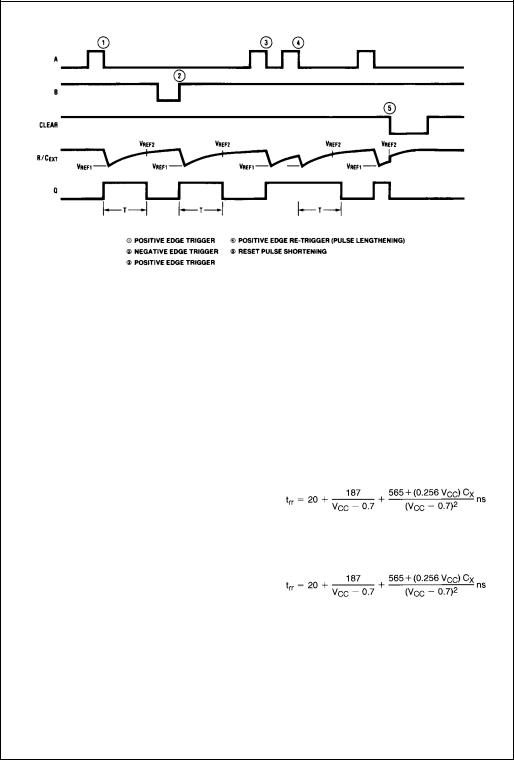
FIGURE 1.
TRIGGER OPERATION
As shown in Figure 1 and the Logic Diagram before an input trigger occurs, the one-shot is in the quiescent state with the Q output LOW, and the timing capacitor CEXT completely charged to VCC. When the trigger input A goes from VCC to GND (while inputs B and clear are held to VCC) a valid trigger is recognized, which turns on comparator C1 and N-Channel transistor N11. At the same time the output latch is set. With transistor N1 on, the capacitor CEXT rapidly discharges toward GND until VREF1 is reached. At this point the output of comparator C1 changes state and transistor N1 turns OFF. Comparator C1 then turns OFF while at the same time comparator C2 turns on. With transistor N1 OFF, the capacitor CEXT begins to charge through the timing resistor, REXT, toward VCC. When the voltage across CEXTequals VREF2, comparator C2 changes state causing the output latch to reset (Q goes LOW) while at the same time disabling comparator C2. This ends the timing cycle with the one-shot in the quiescent state, waiting for the next trigger.
A valid trigger is also recognized when trigger input B goes from GND to VCC (while input A is at GND and input clear is at VCC2.)
It should be noted that in the quiescent state CEXTis fully charged to VCC causing the current through resistor REXT to be zero. Both comparators are “OFF” with the total device current due only to reverse junction leakages. An added feature of the MM74HC423A is that the output latch is set via the input trigger without regard to the capacitor voltage. Thus, propagation delay from trigger to Q is independent of the value of CEXT, REXT, or the duty cycle of the input waveform.
RETRIGGER OPERATION
The MM74HC423A is retriggered if a valid trigger occurs 3 followed by another trigger 4 before the Q output has returned to the quiescent (zero) state. Any retrigger, after the timing node voltage at pin or has begun to rise from VREF1, but has not yet reached VREF2, will cause an increase in output pulse width T. When a valid retrigger is initiated 4, the voltage at the R/CEXT pin will again drop to VREF1 before progressing along the RC charging curve toward VCC. The Q output will remain high until time T, after the last valid retrigger.
Because the trigger-control circuit flip-flop resets shortly after CX has discharged to the reference voltage of the lower reference circuit, the minimum retrigger time, trr is a function of internal propagation delays and the discharge time of CX:
Another removal/retrigger time occurs when a short clear pulse is used. Upon receipt of a clear, the one shot must charge the capacitor up to the upper trip point before the one shot is ready to receive the next trigger. This time is dependent on the capacitor used and is approximately:
MM74HC423A
3 |
www.fairchildsemi.com |
 Loading...