


MM74HC251MX
Fairchild Semiconductor MM74HC251MX, MM74HC251SJX, MM74HC251N, MM74HC251MTCX, MM74HC251M Datasheet
...
September 1983
Revised February 1999
MM74HC251 8-Channel 3-STATE Multiplexer
© 1999 Fairchild Semiconductor Corporation DS005328.prf www.fairchildsemi.com
MM74HC251
8-Channel 3-STATE Multiplexer
General Description
The MM74HC251 8-channel digital multiplexer with 3STATE outputs utilizes advanced silicon-gate CMOS technology. Along with the high noise immunity and low power
consumption of standar d CMOS integrated c ircuits, it possesses the ability to drive 10 LS-TTL loads. The large output drive capability and 3-STATE feature make this part
ideally suited for interfacing with bus lines in a bus oriented
system.
This multiplexer features both true (Y) and complement
(W) outputs as well as a STROBE input. The STROBE
must be at a low logic level to enable this device. When the
STROBE input is HIGH, both outputs are in the high
impedance state. When e nabled, address information on
the data select inputs determines which data input is routed
to the Y and W outputs. The 74HC logic family is speed,
function, as well as pinout co mpatible with the standard
74LS logic family. All inputs are protected from damage
due to static discharge by internal diode clamps to V
CC
and
ground.
Features
■ Typical propagation delay
Data select to Y: 26 ns
■ Wide supply range: 2–6V
■ Low power supply quiescent current:
80 µA maximum (74 HC)
■ 3-STATE outputs for interface to bus oriented
systems
Ordering Code:
Devices also available in Tape and Reel. Specify by appending the suffix letter “X” to the ordering code.
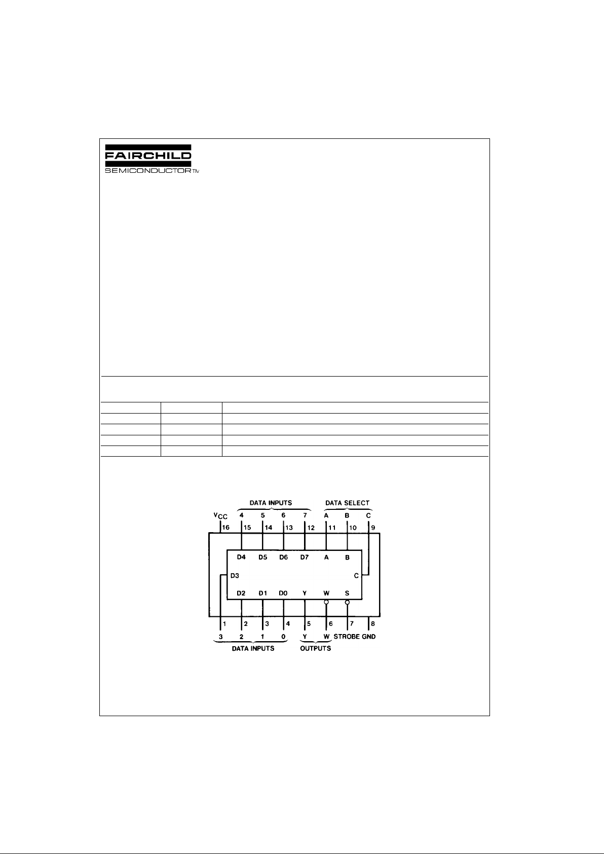
Connection Diagram
Pin Assignments for DIP, SOIC, SOP and TSSOP
Top View
Order Number Package Number Package Description
MM74HC251M M16A 16-Lead Small Outline Integrated Circuit (SOIC), JEDEC MS-120, 0.150” Narrow
MM74HC251SJ M16D 16-Lead Small Outline Package (SOP), EIAJ TYPE II, 5.3mm Wide
MM74HC251MTC MTC16 16-Lead Thin Shrink Small Outline Package (TSSOP), JEDEC MO-153, 4.4mm Wide
MM74HC251N N16E 16-Lead Plastic Dual-In-Line Package (PDIP), JEDEC MS-001, 0.300” Wide
www.fairchildsemi.com 2
MM74HC251
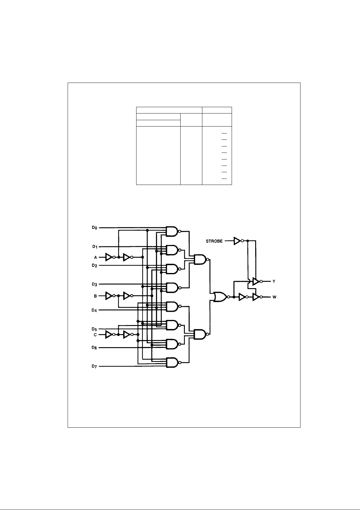
Truth Table
H = HIGH Logic Level, L = LOW Logic Level
X = Irrelevant, Z = High Impedance (o ff)
D0, D1. . . D7 = The level of the respective D input
Logic Diagram
Inputs Outputs
Select Strobe
YW
CBA S
XXX H ZZ
L L L L D0 D0
L L H L D1 D1
L H L L D2 D2
L H H L D3 D3
H L L L D4 D4
H L H L D5 D5
H H L L D6 D6
HHH L D7D7
3 www.fairchildsemi.com
MM74HC251
Absolute Maximum Ratings(Note 1)
(Note 2)
Recommended Operating
Conditions
Note 1: Absolute Maximum Rati ngs are tho se values b eyond which d am-
age to the device may occur.
Note 2: Unless otherwise specified all voltages are referenced to gro und.
Note 3: Power Dissipation temperature de rating — p lastic “N” p ackage: −
12 mW/°C from 65°C to 85°C.
DC Electrical Characteristics (Note 4)
Note 4: For a power supply o f 5V ±10% the worst case output voltages (VOH, and VOL) occur for HC at 4 .5V. Thus the 4.5V values s hould be us ed wh en
designing with this supply. Worst case V
IH
and VIL occur at V
CC
= 5.5V and 4.5V respectively. (The VIH value at 5.5V is 3.85V.) The worst case leakage cur-
rent (I
IN
, ICC, and IOZ) occur for CMOS at the higher voltage and so the 6.0V values s hould be used.
Supply Voltage (VCC) −0.5 to +7.0V
DC Input Voltage (V
IN
) −1.5 to V
CC
+1.5V
DC Output Voltage (V
OUT
) −0.5 to V
CC
+0.5V
Clamp Diode Current (I
IK
, IOK) ±20 mA
DC Output Current, per pin (I
OUT
) ±25 mA
DC V
CC
or GND Current, per pin (ICC) ±50 mA
Storage Temperature Range (T
STG
) −65°C to +150°C
Power Dissipation (P
D
)
(Note 3) 600 mW
S.O. Package only 500 mW
Lead Temperature (T
L
)
(Soldering 10 seconds) 260°C
Min Max Units
Supply Voltage (V
CC
)26V
DC Input or Output Voltage
(V
IN
, V
OUT
)0V
CC
V
Operating Temperature Range (T
A
) −40 +85 °C
Input Rise or Fall Times
(t
r
, tf) V
CC
= 2.0V 1000 ns
V
CC
= 4.5V 500 ns
V
CC
= 6.0V 400 ns
Symbol Parameter Conditions
V
CC
TA = 25°CTA = −40 to 85°CTA = −55 to 125°C
Units
Typ Guaranteed Limits
V
IH
Minimum HIGH Level 2.0V 1.5 1.5 1.5 V
Input Voltage 4.5V 3.15 3.15 3.15 V
6.0V 4.2 4.2 4.2 V
V
IL
Maximum LOW Level 2.0V 0.5 0.5 0.5 V
Input Voltage 4.5V 1.35 1.35 1.35 V
6.0V 1.8 1.8 1.8 V
V
OH
Minimum HIGH Level V
IN
= VIH or V
IL
Output Voltage |I
OUT
| ≤ 20 µA 2.0V 2.0 1.9 1.9 1.9 V
4.5V 4.5 4.4 4.4 4.4 V
6.0V 6.0 5.9 5.9 5.9 V
V
IN
= VIH or V
IL
|I
OUT
| ≤ 4.0 mA 4.5V 4.2 3.98 3.84 3.7 V
|I
OUT
| ≤ 5.2 mA 6.0V 5.7 5.48 5.34 5.2 V
V
OL
Maximum LOW Level V
IN
= VIH or V
IL
Output Voltage |I
OUT
| ≤ 20 µA 2.0V 0 0.1 0.1 0.1 V
4.5V 0 0.1 0.1 0.1 V
6.0V 0 0.1 0.1 0.1 V
V
IN
= VIH or V
IL
|I
OUT
| ≤ 4.0 mA 4.5V 0.2 0.26 0.33 0.4 V
|I
OUT
| ≤ 5.2 mA 6.0V 0.2 0.26 0.33 0.4 V
I
IN
Maximum Input V
IN
= VCC or GND 6.0V ±0.1 ±1.0 ±1.0 µA
Current
I
OZ
Maximum 3-STATE Strobe = V
CC
6.0V ±0.5 ±5 ±10 µA
Leakage Current V
OUT
= VCC or GND
I
CC
Maximum Quiescent V
IN
= VCC or GND 6.0V 8.0 80 160 µA
Supply Current I
OUT
= 0 µA
 Loading...