


MM74C74MX

October 1987
Revised January 1999
MM74C74 Dual D-Type Flip-Flop
© 1999 Fairchild Semiconductor Corporation DS005885.prf www.fairchildsemi.com
MM74C74
Dual D-Type Flip-Flop
General Description
The MM74C74 dual D- type fli p-f lop i s a m on ol ithic comple-
mentary MOS (CMOS ) integrated circuit constructed w ith
N- and P-channel enhancement transisto rs. Each flip-flop
has independent data, preset, clear and clock inputs and Q
and Q
outputs. The logic level pres ent at the data input is
transferred to the output during the positive going transition
of the clock pulse. Preset or clear is independent of the
clock an d acc om pl i s hed by a low l evel at t he pr e set or c lea r
input.
Features
■ Supply voltage range: 3V to 15V
■ Tenth power TTL compatible: Drive 2 LPT
2
L loads
■ High noise immunity: 0.45 V
CC
(typ.)
■ Low power: 50 nW (typ.)
■ Medium speed operation: 10 MHz (typ.) with 10V
supply
Applications
• Automotive
• Data terminals
• Instrumentation
• Medical electronics
• Alarm system
• Industrial electronics
• Remote metering
• Computers
Ordering Code:
Devices also available in Tape and Reel. Specify by appending the suffix letter “X” to the ordering code.
Connection Diagram
Pin Assignments for DIP and SOIC
Note: A logic “0” on clear s et s Q t o logic “0”.
A logic “0” on preset se ts Q to logic “1”.
Top View
Truth Table
Note 1: No change in output from previous state.
Order Number Package Number Package Description
MM74C74M M14A 14-Lead Small Outline Integrated Circuit (SOIC), JEDEC MS-120, 0.150” Narrow
MM74C74N N14A 14-Lead Plastic Dual-In-Line Package (PDIP), JEDEC MS-001, 0.300” Wide
Preset Clear Q
n
Q
n
0000
0110
1001
11Q
n
(Note 1) Q
n
(Note 1)
www.fairchildsemi.com 2
MM74C74
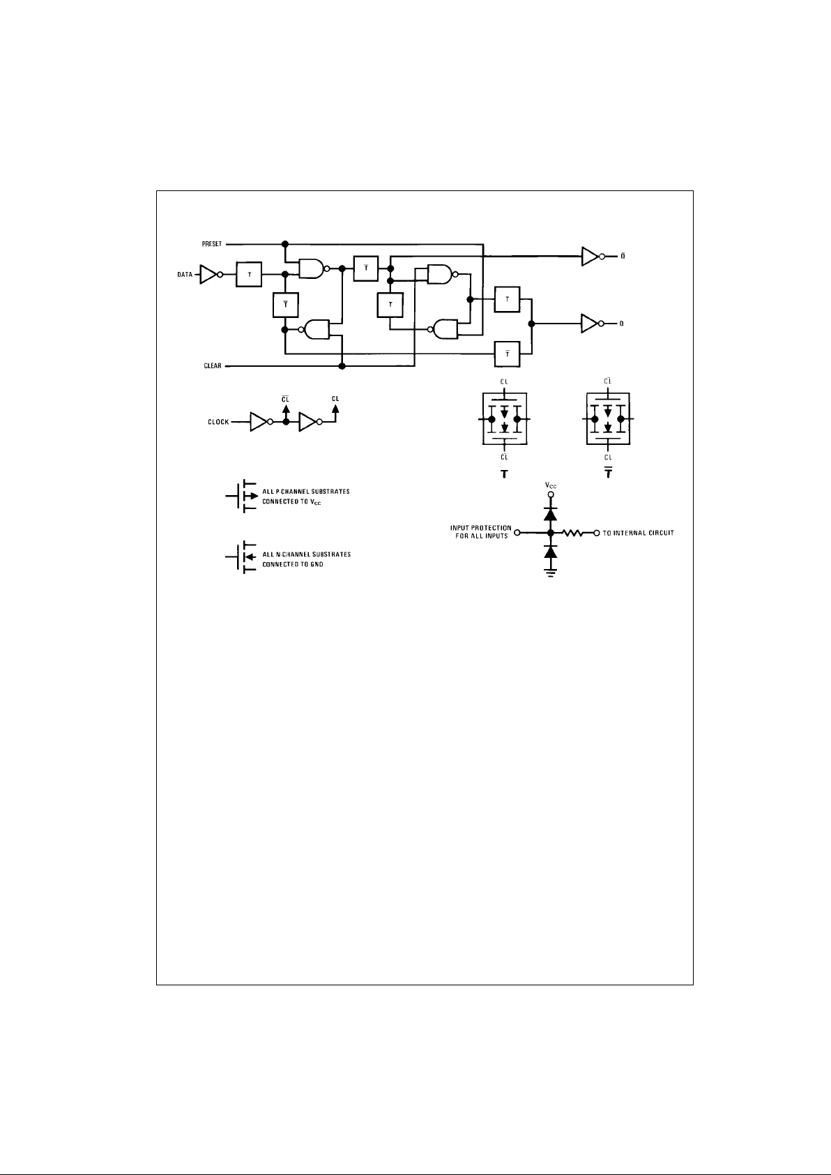
Logic Diagram
3 www.fairchildsemi.com
MM74C74
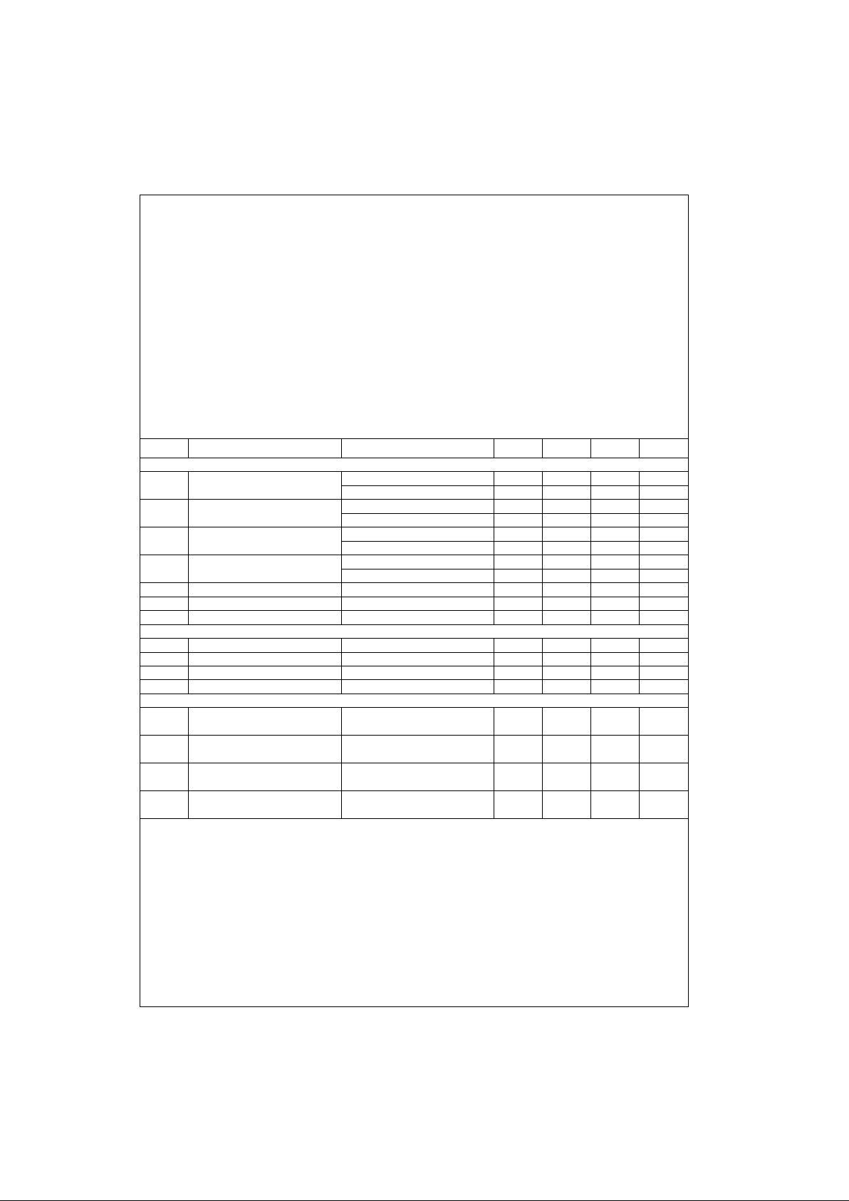
Absolute Maximum Ratings(Note 2)
Note 2: “Absolute Maximum Rat ings” are tho se values beyond which the
safety of the device cannot be guaranteed. Exc ept for “ Operating Tempera-
ture Range” they are not mea nt to imply that the devices sh ould be oper-
ated at these limits. The table of “Electrical Characteristics” provides
conditions for actual device o peration.
DC Electrical Characteristics
Min/Max limits apply across temperature range unless otherwise noted
Voltage at Any Pin (Note 2) −0.3V to V
CC
+0.3V
Operating Temperature Range −40°C to +85°C
Storage Temperature Range −65°C to +150°C
Power Dissipation
Dual-In-Line 700 mW
Small Outline 500 mW
Lead Temperature
(Soldering, 10 seconds ) 260°C
Operating V
CC
Range 3V to 15V
V
CC
(Max) 18V
Symbol Parameter Conditions Min Typ Max Units
CMOS TO CMOS
V
IN(1)
Logical “1” Input Voltage V
CC
= 5V 3.5 V
V
CC
= 10V 80 V
V
IN(0)
Logical “0” Input Voltage V
CC
= 5V 1.5 V
V
CC
= 10V 2.0 V
V
OUT(1)
Logical “1” Output Voltage V
CC
= 5V 4.5 V
V
CC
= 10V 9.0 V
V
OUT(0)
Logical “0” Output Voltage V
CC
= 5V 0.5 V
V
CC
= 10V 1.0 V
I
IN(1)
Logical “1” Input Current V
CC
= 15V 1.0 µA
I
IN(0)
Logical “0” Input Current V
CC
= 15V −1.0 µA
I
CC
Supply Current V
CC
= 15V 0.05 60 µA
CMOS/LPTTL INTERFACE
V
IN(1)
Logical “1” Input Voltage V
CC
= 4.75V V
CC
−1.5
V
IN(0)
Logical “0” Input Voltage V
CC
= 4.75V 0.8 V
V
OUT(1)
Logical “1” Output Voltage V
CC
= 4.75V, I
D
= −360 µA2.4 V
V
OUT(0)
Logical “0” Output Voltage V
CC
= 4.75V, I
D
= 360 µA0.4V
OUTPUT DRIVE (See Family Characteristics Data Sheet)
I
SOURCE
Output Source Current V
CC
= 5V, V
IN(0)
= 0V −1.75 mA
T
A
= 25°C, V
OUT
= 0V
I
SOURCE
Output Source Current V
CC
= 10V, V
IN(0)
= 0V −8.0 mA
T
A
= 25°C, V
OUT
= 0V
I
SINK
Output Sink Current V
CC
= 5V, V
IN(1)
= 5V 1.75 mA
T
A
= 25°C, V
OUT
= V
CC
I
SINK
Output Sink Current V
CC
= 10V, V
IN(1)
= 10V 8.0 mA
T
A
= 25°C, V
OUT
= V
CC
 Loading...