


October 1987
Revised July 1999
MM74C240 • MM74C244
Inverting • Non-Inverting Octal Buffer and Line Driver with 3-STATE Outputs
General Description
The MM74C240 and MM74C244 octal buffers and line drivers are monolithic complementary MOS (CMOS) integrated circuits with 3-STATE outputs. These outputs have been specially designed to drive highly capacitive loads such as bus-oriented systems. These devices have a fan out of 6 low power Schottky loads. A high logic level on the output disable control input G makes the outputs go into the high impedance state.
Features
■Wide supply voltage range (3V to 15V)
■High noise immunity (0.45 VCC typ)
■Low power consumption
■High capacitive load drive capability
■3-STATE outputs
■Input protection
■TTL compatibility
■20-pin dual-in-line package
■High speed 25 ns (typ.) @ 10V, 50 pF (MM74C244)
Ordering Code:
Order Number |
Package Number |
Package Description |
|
|
|
MM74C240WM |
M20B |
20-Lead Small Outline Integrated Circuit (SOIC), JEDEC MS-013, 0.300” Wide Body |
|
|
|
MM74C240N |
N20A |
20-Lead Plastic Dual-In-Line Package (PDIP), JEDEC MS-001, 0.300” Wide |
|
|
|
MM74C244WM |
M20B |
20-Lead Small Outline Integrated Circuit (SOIC), JEDEC MS-013, 0.300” Wide Body |
|
|
|
MM74C244N |
N20A |
20-Lead Plastic Dual-In-Line Package (PDIP), JEDEC MS-001, 0.300” Wide |
|
|
|
Devices also available in Tape and Reel. Specify by appending suffix letter “X” to the ordering code.
Connection Diagrams
Pin Assignments for DIP and SOIC
MM74C240 |
MM74C244 |
(Top View) |
(Top View) |
Outputs STATE-3 with Driver Line and Buffer Octal Inverting-Non • Inverting MM74C244 • MM74C240
© 1999 Fairchild Semiconductor Corporation |
DS005905 |
www.fairchildsemi.com |
MM74C240 • MM74C244
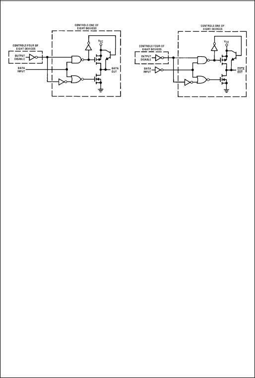
Logic Diagrams
MM74C240
Truth Tables
|
MM74C240 |
|
|
|
|
ODA |
IA |
OA |
|
|
|
1 |
X |
Z |
1 |
X |
Z |
0 |
0 |
1 |
0 |
1 |
0 |
|
|
|
|
|
ODB |
IB |
OB |
|
|
|
|
|
|
|
1 |
X |
Z |
|
|
1 |
X |
Z |
|
|
0 |
0 |
1 |
|
|
0 |
1 |
0 |
|
|
|
|
|
1 |
= HIGH |
|
|
|
0 |
= LOW |
|
|
|
X |
= Don’t Care |
|
|
|
Z |
= 3-STATE |
|
|
|
MM74C244
MM74C244
ODA |
IA |
OA |
|
|
|
1 |
X |
Z |
1 |
X |
Z |
0 |
0 |
0 |
0 |
1 |
1 |
|
|
|
ODB |
IB |
OB |
|
|
|
1 |
X |
Z |
1 |
X |
Z |
0 |
0 |
0 |
0 |
1 |
1 |
|
|
|
www.fairchildsemi.com |
2 |

Absolute Maximum Ratings(Note 1)
Voltage at Any Pin |
−0.3V to VCC + 0.3V |
Operating Temperature Range |
−40°C to +85°C |
Storage Temperature Range |
−65°C to +150°C |
Power Dissipation |
|
Dual-In-Line |
700 mW |
Small Outline |
500 mW |
Operating VCC Range |
3V to 15V |
Absolute Maximum VCC |
18V |
Lead Temperature |
260°C |
(Soldering, 10 seconds) |
Note 1: “Absolute Maximum Ratings” are those values beyond which the safety of the device cannot be guaranteed. Except for “Operating Range” they are not meant to imply that the devices should be operated at these limits. The Electrical Characteristics table provides conditions for actual device operation.
DC Electrical Characteristics
Min/Max limits apply across temperature range, unless otherwise noted
Symbol |
Parameter |
Conditions |
Min |
Typ |
Max |
Units |
|
|
|
|
|
|
|
CMOS TO CMOS |
|
|
|
|
|
|
|
|
|
|
|
|
|
VIN(1) |
Logical “1” Input Voltage |
VCC = 5V |
3.5 |
|
|
V |
|
|
VCC = 10V |
8.0 |
|
|
V |
VIN(0) |
Logical “0” Input Voltage |
VCC = 5V |
|
|
1.5 |
V |
|
|
VCC = 10V |
|
|
2.0 |
V |
VOUT(1) |
Logical “1” Output Voltage |
VCC = 5V, I O = −10 μA |
4.5 |
|
|
V |
|
|
VCC = 10V, IO = −10 μA |
9.0 |
|
|
V |
VOUT(0) |
Logical “0” Output Voltage |
VCC = 5V, I O = 10 μA |
|
|
0.5 |
V |
|
|
VCC = 10V, IO = 10 μA |
|
|
1.0 |
V |
IOZ |
3-STATE Output Current |
VCC = 10V, OD = VIH |
|
|
±10 |
μA |
IIN(1) |
Logical “1” Input Current |
VCC = 15V, VIN = 15V |
|
0.005 |
1.0 |
μA |
IIN(0) |
Logical “0” Input Current |
VCC = 15V, VIN = 0V |
−1.0 |
−0.005 |
|
μA |
ICC |
Supply Current |
VCC = 15V |
|
0.05 |
300 |
μA |
CMOS/LPTTL INTERFACE |
|
|
|
|
|
|
|
|
|
|
|
|
|
VIN(1) |
Logical “1” Input Voltage |
VCC = 4.75V |
VCC − 1.5 |
|
|
V |
VIN(0) |
Logical “0” Input Voltage |
VCC = 4.75V |
|
|
0.8 |
V |
VOUT(1) |
Logical “1” Output Voltage |
VCC = 4.75V, IO = −450 μA |
VCC − 0.4 |
|
|
V |
|
|
VCC = 4.75V, IO = −2.2 mA |
2.4 |
|
|
V |
VOUT(0) |
Logical “0” Output Voltage |
VCC = 4.75V, IO = 2.2 mA |
|
|
0.4 |
V |
OUTPUT DRIVE (See Family Characteristics Data Sheet) (Short Circuit Current) |
|
|
|
|
||
|
|
|
|
|
|
|
ISOURCE |
Output Source Current |
VCC = 5V, V OUT = 0V |
−14 |
−30 |
|
mA |
|
(P-Channel) |
TA = 25°C |
|
|
|
|
|
|
VCC = 10V, VOUT = 0V |
−36 |
−70 |
|
mA |
|
|
TA = 25°C |
|
|
|
|
ISINK |
Output Sink Current |
VCC = 5V, V OUT = VCC |
12 |
20 |
|
mA |
|
(N-Channel) |
TA = 25°C |
|
|
|
|
|
|
VCC = 10V, VOUT = VCC |
48 |
70 |
|
mA |
|
|
TA = 25°C |
|
|
|
|
MM74C244 • MM74C240
3 |
www.fairchildsemi.com |
 Loading...