Fairchild Semiconductor 74LVTH574MSAX, 74LVTH574MSA, 74LVTH574WMX, 74LVTH574WM, 74LVTH574SJX Datasheet
...
March 1999
Revised March 1999
74LVT574 • 74LVTH574
Low Voltage Octal D-Type Flip-Flop with 3-STATE Outputs
General Description
The LVT574 and LVTH574 are high-speed, low-power octal D-type flip-flop featuring separate D-type inputs for each flip-flop and 3-STATE outputs for bus-oriented applications. A buffered Clock (CP) and Output Enable (OE) are common to all flip-flops.
The LVTH574 data inputs include bushold, eliminating the need for external pull-up resistors to hold unused inputs.
These octal flip-flops are designed for low-voltage (3.3V) VCC applications, but with the capability to provide a TTL interface to a 5V environment. The LVT574 and LVTH574 are fabricated with an advanced BiCMOS technology to achieve high speed operation similar to 5V ABT while maintaining a low power dissipation.
Features
■Input and output interface capability to systems at 5V VCC
■Bushold data inputs eliminate the need for external pullup resistors to hold unused inputs (74LVTH574), also available without bushold feature (74LVT574).
■Live insertion/extraction permitted
■Power Up/Down high impedance provides glitch-free bus loading
■Outputs source/sink −32 mA/+64 mA
■Functionally compatible with the 74 series 574
■Latch-up performance exceeds 500 mA
Ordering Code:
Order Number |
Package Number |
Package Description |
|
|
|
74LVT574WM |
M20B |
20-Lead Small Outline Integrated Circuit (SOIC), JEDEC MS-013, .300” Wide |
|
|
|
74LVT574SJ |
M20D |
20-Lead Small Outline Package (SOP), EIAJ TYPE II 5.3mm Wide |
|
|
|
74LVT574MTC |
MTC20 |
20-Lead Thin Shrink Small Outline Package (TSSOP), JEDEC MO-153, 4.4mm Wide |
|
|
|
74LVT574MSA |
MSA20 |
20-Lead Shrink Small Outline Package (SSOP), EIAJ TYPE II, 5.3mm Wide |
|
|
|
74LVTH574WM |
M20B |
20-Lead Small Outline Integrated Circuit (SOIC), JEDEC MS-013, .300” Wide |
|
|
|
74LVTH574SJ |
M20D |
20-Lead Small Outline Package (SOP), EIAJ TYPE II 5.3mm Wide |
|
|
|
74LVTH574MTC |
MTC20 |
20-Lead Thin Shrink Small Outline Package (TSSOP), JEDEC MO-153, 4.4mm Wide |
|
|
|
74LVTH574MSA |
MSA20 |
20-Lead Shrink Small Outline Package (SSOP), EIAJ TYPE II, 5.3mm Wide |
|
|
|
Device also available in Tape and Reel. Specify by appending suffix letter “X” to the ordering code.
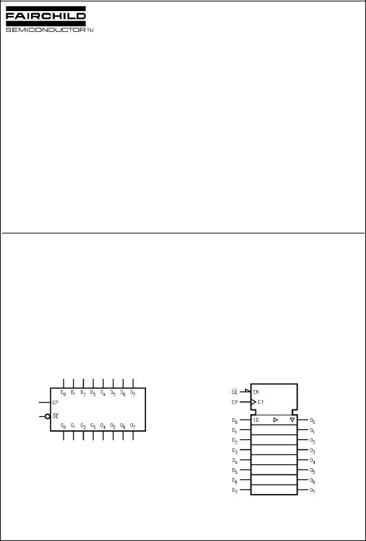
Logic Symbols
IEEE/IEC
Outputs STATE-3 with Flop-Flip Type-D Octal Voltage Low 74LVTH574 • 74LVT574
© 1999 Fairchild Semiconductor Corporation |
DS012451.prf |
www.fairchildsemi.com |

74LVT574 • 74LVTH574
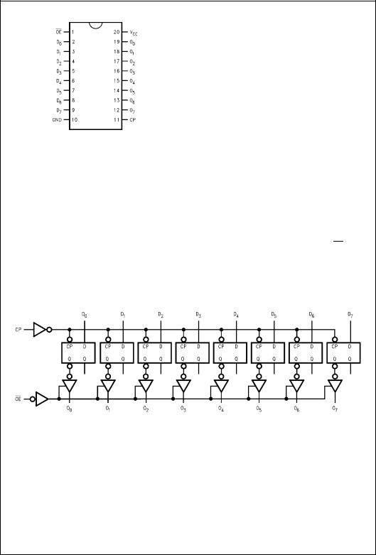
Connection Diagram
Functional Description
The LVT574 and LVTH574 consist of eight edge-triggered flip-flops with individual D-type inputs and 3-STATE true outputs. The buffered clock and buffered Output Enable are common to all flip-flops. The eight flip-flops will store the state of their individual D-type inputs that meet the setup and hold time requirements on the LOW-to-HIGH
Logic Diagram
Pin Descriptions
|
Pin Names |
Description |
|
|
|
|
|
|
D0–D7 |
Data Inputs |
|
|
CP |
Clock Pulse Input |
|
|
|
3-STATE Output Enable Input |
|
|
OE |
|
|
|
O0–O7 |
3-STATE Outputs |
|
Truth Table |
|
||
|
|
Inputs |
|
|
|
Outputs |
|
|
|
|
|
|
|
|
|
|
Dn |
|
CP |
|
OE |
|
On |
|
H |
|
|
|
L |
|
H |
|
L |
|
|
|
L |
|
L |
|
X |
|
L |
|
L |
|
Oo |
|
X |
|
X |
|
H |
|
Z |
|
|
|
|
|
|
|
|
H = HIGH Voltage Level |
|
|
|
|
|
||
L = LOW Voltage Level |
|
|
|
|
|
||
X = Immaterial |
|
|
|
|
|
||
Z = High Impedance |
|
|
|
|
|
||
= LOW-to-HIGH Transition
Oo = Previous Oo before HIGH to LOW of CP
Clock (CP) transition. With the Output Enable (OE) LOW, the contents of the eight flip-flops are available at the outputs. When the OE is HIGH, the outputs go to the high impedance state. Operation of the OE input does not affect the state of the flip-flops.
Please note that this diagram is provided only for the understanding of logic operations and should not be used to estimate propagation delays.
www.fairchildsemi.com |
2 |

Absolute Maximum Ratings(Note 1)
Symbol |
Parameter |
Value |
|
Conditions |
Units |
|
|
|
|
|
|
VCC |
Supply Voltage |
−0.5 to +4.6 |
|
|
V |
VI |
DC Input Voltage |
−0.5 to +7.0 |
|
|
V |
VO |
DC Output Voltage |
−0.5 to +7.0 |
Output in 3-STATE |
V |
|
|
|
−0.5 to +7.0 |
Output in High or Low State (Note 2) |
||
|
|
|
|||
IIK |
DC Input Diode Current |
−50 |
VI < GND |
|
mA |
IOK |
DC Output Diode Current |
−50 |
VO < GND |
|
mA |
IO |
DC Output Current |
64 |
VO > VCC |
Output at High State |
mA |
|
|
128 |
VO > VCC |
Output at Low State |
|
|
|
|
|||
ICC |
DC Supply Current per Supply Pin |
±64 |
|
|
mA |
IGND |
DC Ground Current per Ground Pin |
±128 |
|
|
mA |
TSTG |
Storage Temperature |
−65 to +150 |
|
|
°C |
Recommended Operating Conditions |
|
|
|
||
Symbol |
Parameter |
Min |
Max |
Units |
|
|
|
|
|
VCC |
Supply Voltage |
2.7 |
3.6 |
V |
VI |
Input Voltage |
0 |
5.5 |
V |
IOH |
High-Level Output Current |
|
−32 |
mA |
IOL |
Low-Level Output Current |
|
64 |
mA |
TA |
Free-Air Operating Temperature |
−40 |
85 |
°C |
t/ V |
Input Edge Rate, VIN = 0.8V–2.0V, VCC = 3.0V |
0 |
10 |
ns/V |
Note 1: Absolute Maximum continuous ratings are those values beyond which damage to the device may occur. Exposure to these conditions or conditions beyond those indicated may adversely affect device reliability. Functional operation under absolute maximum rated conditions is not implied.
Note 2: IO Absolute Maximum Rating must be observed.
DC Electrical Characteristics
|
|
|
VCC |
T A = -40°C to +85°C |
|
|
|||
Symbol |
Parameter |
|
|
|
Units |
Conditions |
|||
Min |
Typ |
Max |
|||||||
(V) |
|||||||||
|
|
|
|
(Note 3) |
|
|
|
||
|
|
|
|
|
|
|
|
||
|
|
|
|
|
|
|
|
|
|
VIK |
Input Clamp Diode Voltage |
2.7 |
|
|
-1.2 |
V |
II = -18 mA |
||
VIH |
Input HIGH Voltage |
2.7–3.6 |
2.0 |
|
|
V |
VO £ 0.1V or |
||
|
|
|
|
|
|
|
|
VO ³ VCC - 0.1V |
|
VIL |
Input LOW Voltage |
2.7–3.6 |
|
|
0.8 |
V |
|||
|
|
|
|||||||
VOH |
Output HIGH Voltage |
2.7–3.6 |
VCC - 0.2 |
|
|
|
IOH = -100 mA |
||
|
|
|
2.7 |
2.4 |
|
|
V |
IOH = -8 mA |
|
|
|
|
3.0 |
2.0 |
|
|
|
IOH = -32 mA |
|
VOL |
Output LOW Voltage |
2.7 |
|
|
0.2 |
|
IOL = 100 mA |
||
|
|
|
2.7 |
|
|
0.5 |
|
IOL = 24 mA |
|
|
|
|
3.0 |
|
|
0.4 |
V |
IOL = 16 mA |
|
|
|
|
3.0 |
|
|
0.5 |
|
IOL = 32 mA |
|
|
|
|
3.0 |
|
|
0.55 |
|
IOL = 64 mA |
|
II(HOLD) |
Bushold Input Minimum Drive |
3.0 |
75 |
|
|
mA |
VI = 0.8V |
||
(Note 4) |
|
|
|
-75 |
|
|
VI = 2.0V |
||
|
|
|
|
|
|
||||
II(OD) |
Bushold Input Over-Drive |
3.0 |
500 |
|
|
mA |
(Note 5) |
||
|
Current to Change State |
|
|
|
|
|
|||
(Note 4) |
|
-500 |
|
|
(Note 6) |
||||
|
|
|
|
|
|
||||
|
|
|
|
|
|
|
|
|
|
II |
Input Current |
3.6 |
|
|
10 |
|
VI = 5.5V |
||
|
|
Control Pins |
3.6 |
|
|
±1 |
mA |
VI = 0V or VCC |
|
|
|
Data Pins |
3.6 |
|
|
-5 |
VI = 0V |
||
|
|
|
|
|
|||||
|
|
|
|
|
|
1 |
|
VI = VCC |
|
IOFF |
Power Off Leakage Current |
0 |
|
|
±100 |
mA |
0V £ VI or VO £ 5.5V |
||
IPU/PD |
Power up/down 3-STATE |
0–1.5V |
|
|
±100 |
mA |
VO = 0.5V to 3.0V |
||
|
Output Current |
|
|
|
|
|
VI = GND or VCC |
||
IOZL |
3-STATE Output Leakage Current |
3.6 |
|
|
-5 |
mA |
VO = 0.5V |
||
IOZH |
3-STATE Output Leakage Current |
3.6 |
|
|
5 |
mA |
VO = 3.0V |
||
74LVTH574 • 74LVT574
3 |
www.fairchildsemi.com |
 Loading...