


June 1991
Revised November 1999
74ACTQ16541
16-Bit Buffer/Line Driver with 3-STATE Outputs
General Description
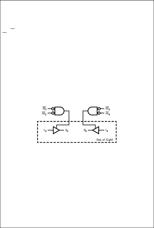
The ACTQ16541 contains sixteen non-inverting buffers with 3-STATE outputs designed to be employed as a memory and address driver, clock driver, or bus oriented transmitter/receiver. The device is byte controlled. Each byte has separate 3-STATE control inputs which can be shorted together for full 16-bit operation.
The ACTQ16541 utilizes Fairchild Quiet Series technology to guarantee quiet output switching and improved dynamic threshold performance. FACT Quiet Series features GTO output control for superior performance.
Features
■Utilizes Fairchild FACT Quiet Series technology
■Guaranteed simultaneous switching noise level and dynamic threshold performance
■Guaranteed pin-to-pin output skew
■Separate control logic for each byte
■16-bit version of the ACTQ541
■Outputs source/sink 24 mA
■Additional specs for Multiple Output Switching
■Output loading specs for both 50 pF and 250 pF loads
Ordering Code:
Order Number |
Package Number |
Package Description |
|
|
|
74ACTQ16541SSC |
MS48A |
48-Lead Small Shrink Outline Package (SSOP), JEDEC MO-118, 0.300” Wide |
|
|
|
74ACTQ16541MTD |
MTD48 |
48-Lead Thin Shrink Small Outline Package (TSSOP), MO-153, 6.1mm Wide |
|
|
|
Device also available in Tape and Reel. Specify by appending suffix letter “X” to the ordering code.
Logic Symbol |
Connection Diagram |
Pin Descriptions
|
Pin Names |
Description |
|
|
|
|
|
|
|
n |
Output Enable Input (Active LOW) |
|
OE |
||
|
I0–I15 |
Inputs |
|
|
O0–O15 |
Outputs |
|
FACT , Quiet Series , FACT Quiet Series and GTO are trademarks of Fairchild Semiconductor Corporation
Outputs STATE-3 with Driver Buffer/Line Bit-16 74ACTQ16541
© 1999 Fairchild Semiconductor Corporation |
DS010936 |
www.fairchildsemi.com |
74ACTQ16541
Functional Description
The ACTQ16541 contains sixteen non-inverting buffers with 3-STATE standard outputs. The device is byte controlled with each byte functioning identically, but independent of the other. The control pins can be shorted together to obtain full 16-bit operation. The 3-STATE outputs are controlled by an Output Enable (OEn) input for each byte.
When OEn is LOW, the outputs are in 2-state mode. When
OEn is HIGH, the outputs are in the high impedance mode, but this does not interfere with entering new data into the inputs.
Logic Diagram
Truth Tables
|
|
|
Inputs |
|
Outputs |
||
|
|
|
|
|
|
||
|
|
|
|
|
|
|
|
OE1 |
|
OE2 |
I0–I7 |
O0–O7 |
|||
|
L |
|
L |
H |
H |
||
|
H |
|
X |
X |
Z |
||
|
X |
|
H |
X |
Z |
||
|
L |
|
L |
L |
L |
||
|
|
|
|
|
|
||
|
|
|
|
|
|
||
|
|
|
Inputs |
|
Outputs |
||
|
|
|
|
|
|||
|
|
|
|
|
|
|
|
OE3 |
|
OE4 |
I8–I15 |
O8–O15 |
|||
|
L |
|
L |
H |
H |
||
|
H |
|
X |
X |
Z |
||
|
X |
|
H |
X |
Z |
||
|
L |
|
L |
L |
L |
||
|
|
|
|
|
|
|
|
H = HIGH Voltage Level
L = LOW Voltage Level
X = Immaterial
Z = High Impedance
www.fairchildsemi.com |
2 |

Absolute Maximum Ratings(Note 1) |
|
|
Recommended Operating |
|
|||||||||||||||
Supply Voltage (VCC) |
− 0.5V to +7.0V |
|
Conditions |
|
|
|
|
|
|
|
|||||||||
DC Input Diode Current (IIK) |
|
|
|
|
|
|
Supply Voltage (V |
|
) |
|
|
|
4.5V to 5.5V |
||||||
VI = − 0.5V |
|
|
− 20 mA |
|
|
|
|
|
|
|
CC |
|
|
|
|
|
|||
|
|
|
|
Input Voltage (V ) |
|
|
|
|
|
|
0V to V |
||||||||
|
|
|
|
|
|
|
|
|
|
|
|
I |
|
|
|
|
|
|
CC |
VI = VCC + 0.5V |
|
|
+20 mA |
|
|
Output Voltage (V |
O |
) |
|
|
|
|
0V to V |
||||||
|
|
|
|
|
|
|
|
|
|
|
|
|
|
|
|
|
|
CC |
|
DC Output Diode Current (IOK) |
|
|
|
|
|
|
Operating Temperature (T ) |
|
− 40° C to +85° C |
||||||||||
VO = − 0.5V |
|
|
− 20 mA |
|
|
|
|
|
|
|
|
|
A |
|
|
|
|||
|
|
|
|
Minimum Input Edge Rate (∆ V/∆ t) |
|
|
125 mV/ns |
||||||||||||
VO = VCC + 0.5V |
|
|
+20 mA |
|
|
VIN from 0.8V to 2.0V |
|
|
|
||||||||||
DC Output Voltage (VO) |
− 0.5V to VCC + 0.5V |
|
|
VCC @ 4.5V, 5.5V |
|
|
|
|
|
||||||||||
DC Output Source/Sink Current (IO) |
|
|
± 50 mA |
|
Note 1: Absolute maximum ratings are those values beyond which damage |
||||||||||||||
DC VCC or Ground Current |
|
|
|
|
|
to the device may occur. The databook specifications should be met, with- |
|||||||||||||
|
|
|
|
|
out exception to ensure that the system design is reliable over its power |
||||||||||||||
per Output Pin |
|
|
± 50 mA |
|
|||||||||||||||
|
|
|
supply, temperature, and output/input loading variables. Fairchild does not |
||||||||||||||||
Storage Temperature |
− 65° C to +150° C |
|
recommend operation of FACT circuits outside databook specifications. |
||||||||||||||||
|
|
|
|
|
|
|
|
|
|
|
|
|
|
||||||
DC Electrical Characteristics |
|
|
|
|
|
|
|
|
|
|
|
|
|
|
|
|
|||
|
|
|
|
|
|
|
|
|
|
|
|
|
|
|
|||||
Symbol |
Parameter |
|
|
VCC |
|
|
TA = +25° C |
|
TA = − 40° C to +85° C |
|
Units |
Conditions |
|||||||
|
|
|
|
(V) |
|
Typ |
|
|
Guaranteed Limits |
|
|
|
|
||||||
|
|
|
|
|
|
|
|
|
|
|
|
|
|
|
|
|
|
|
|
VIH |
Minimum HIGH |
|
|
4.5 |
|
|
1.5 |
|
|
2.0 |
|
|
|
|
2.0 |
|
V |
VOUT = 0.1V |
|
|
Input Voltage |
|
|
5.5 |
|
|
1.5 |
|
|
2.0 |
|
|
|
|
2.0 |
|
or VCC − |
0.1V |
|
|
|
|
|
|
|
|
|
|
|
|
|
|
|||||||
VIL |
Maximum LOW |
|
|
4.5 |
|
|
1.5 |
|
|
0.8 |
|
|
|
|
0.8 |
|
V |
VOUT = 0.1V |
|
|
Input Voltage |
|
|
5.5 |
|
|
1.5 |
|
|
0.8 |
|
|
|
|
0.8 |
|
or VCC − |
0.1V |
|
|
|
|
|
|
|
|
|
|
|
|
|
|
|||||||
VOH |
Minimum HIGH |
|
|
4.5 |
|
4.49 |
|
4.4 |
|
|
|
|
4.4 |
|
V |
IOUT = − |
50 µ A |
||
|
Output Voltage |
|
|
5.5 |
|
5.49 |
|
5.4 |
|
|
|
|
5.4 |
|
|||||
|
|
|
|
|
|
|
|
|
|
|
|
|
|||||||
|
|
|
|
|
|
|
|
|
|
|
|
|
|
|
|
|
|
|
|
|
|
|
|
|
|
|
|
|
|
|
|
|
|
|
|
|
|
VIN = VIL or VIH |
|
|
|
|
|
4.5 |
|
|
|
|
3.86 |
|
|
3.76 |
|
V |
IOH = − 24 mA |
||||
|
|
|
|
5.5 |
|
|
|
|
4.86 |
|
|
4.76 |
|
|
IOH = − 24 mA (Note 2) |
||||
VOL |
Maximum LOW |
|
|
4.5 |
0.001 |
|
0.1 |
|
|
|
|
0.1 |
|
V |
IOUT = 50 µ A |
||||
|
Output Voltage |
|
|
5.5 |
0.001 |
|
0.1 |
|
|
|
|
0.1 |
|
||||||
|
|
|
|
|
|
|
|
|
|
|
|
||||||||
|
|
|
|
|
|
|
|
|
|
|
|
|
|
|
|
|
|
|
|
|
|
|
|
|
|
|
|
|
|
|
|
|
|
|
|
|
|
VIN = VIL or VIH |
|
|
|
|
|
4.5 |
|
|
|
|
0.36 |
|
|
0.44 |
|
V |
IOL = 24 mA |
||||
|
|
|
|
5.5 |
|
|
|
|
0.36 |
|
|
0.44 |
|
|
IOL = 24 mA (Note 2) |
||||
IOZ |
Maximum 3-STATE |
|
|
5.5 |
|
|
|
|
± |
0.5 |
|
|
± |
5.0 |
|
µ A |
VI = VIL, VIH |
||
|
Leakage Current |
|
|
|
|
|
|
|
|
|
VO = VCC, GND |
||||||||
|
|
|
|
|
|
|
|
|
|
|
|
|
|
|
|
|
|||
IIN |
Maximum Input Leakage Current |
|
|
5.5 |
|
|
|
|
± |
0.1 |
|
|
± |
1.0 |
|
µ A |
VI = VCC, GND |
||
ICCT |
Maximum ICC/Input |
|
|
5.5 |
|
|
0.6 |
|
|
|
|
|
|
|
1.5 |
|
mA |
VI = VCC − 2.1V |
|
ICC |
Max Quiescent Supply Current |
|
|
5.5 |
|
|
|
|
|
8.0 |
|
|
|
80.0 |
|
µ A |
VIN = VCC or GND |
||
IOLD |
Minimum Dynamic |
|
|
5.5 |
|
|
|
|
|
|
|
|
|
|
75 |
|
mA |
VOLD = 1.65V Max |
|
IOHD |
Output Current (Note 3) |
|
|
|
|
|
|
|
|
|
|
|
− 75 |
|
mA |
VOHD = 3.85V Min |
|||
|
|
|
|
|
|
|
|
|
|
|
|
|
|||||||
VOLP |
Quiet Output |
|
|
5.0 |
|
|
0.5 |
|
|
0.8 |
|
|
|
|
|
|
V |
Figure 1, Figure 2 |
|
|
Maximum Dynamic VOL |
|
|
|
|
|
|
|
|
|
|
|
|
(Note 5)(Note 6) |
|||||
|
|
|
|
|
|
|
|
|
|
|
|
|
|
|
|
|
|||
VOLV |
Quiet Output |
|
|
5.0 |
|
− |
0.5 |
− |
1.0 |
|
|
|
|
|
V |
Figure 1, Figure 2 |
|||
|
Minimum Dynamic VOL |
|
|
|
|
|
|
|
|
(Note 5)(Note 6) |
|||||||||
|
|
|
|
|
|
|
|
|
|
|
|
|
|
|
|
|
|||
VOHP |
Maximum |
|
|
5.0 |
V |
OH |
+ |
V |
OH |
+ |
|
|
|
|
|
V |
Figure 1, Figure 2 |
||
|
Overshoot |
|
|
|
|
|
|
|
|
|
|
|
|
(Note 4)(Note 6) |
|||||
|
|
|
|
|
|
1.0 |
|
|
1.5 |
|
|
|
|
|
|
|
|||
|
|
|
|
|
|
|
|
|
|
|
|
|
|
|
|
|
|
|
|
VOHV |
Minimum |
|
|
5.0 |
VOH − 1.0 |
VOH − |
1.8 |
|
|
|
|
|
V |
Figure 1, Figure 2 |
|||||
|
VCC Droop |
|
|
|
|
|
|
|
(Note 4)(Note 6) |
||||||||||
|
|
|
|
|
|
|
|
|
|
|
|
|
|
|
|
|
|||
VIHD |
Minimum HIGH Dynamic Input Voltage Level |
|
5.0 |
|
|
1.7 |
|
|
2.0 |
|
|
|
|
|
|
V |
(Note 4)(Note 7) |
||
VILD |
Maximum LOW Dynamic Input Voltage Level |
|
5.0 |
|
|
1.2 |
|
|
0.8 |
|
|
|
|
|
|
V |
(Note 4)(Note 7) |
||
Note 2: All outputs loaded; thresholds associated with output under test.
Note 3: Maximum test duration 2.0 ms; one output loaded at a time.
Note 4: Worst case package.
Note 5: Maximum number of outputs that can switch simultaneously is n. (n − 1) outputs are switched LOW and one output held LOW.
Note 6: Maximum number of outputs that can switch simultaneously is n. (n − 1) outputs are switched HIGH and one output held HIGH.
Note 7: Maximum number of data inputs (n) switching. (n − 1) input switching 0V to 3V. Input under test switching 3V to threshold (VILD).
74ACTQ16541
3 |
www.fairchildsemi.com |
 Loading...