


March 1990
Revised December 1998
74ACTQ827
Quiet Seriesä 10-Bit Buffer/Line Driver with 3-STATE Outputs
General Description
The ACTQ827 10-bit bus buffer provides high performance bus interface buffering for wide data/address paths or buses carrying parity. The 10-bit buffers have NOR output enables for maximum control flexibility. The ACTQ827 utilizes Fairchild Quiet Seriesä technology to guarantee quiet output switching and improved dynamic threshold performance. FACT Quiet Seriesä features GTOä output control and undershoot corrector in addition to a split ground bus for superior performance.
Features
■Guaranteed simultaneous switching noise level and dynamic threshold performance
■Guaranteed pin-to-pin skew AC performance
■Inputs and outputs on opposite sides of package allow easy interface with microprocessors
■Improved latch-up immunity
■Outputs source/sink 24 mA
■Functionally and pin-compatible to AMD’s AM29827
■Has TTL-compatible inputs
Ordering Code:
Order Number |
Package Number |
Package Description |
|
|
|
74ACTQ827SC |
M24B |
24-Lead Small Outline Integrated Circuit (SOIC), JEDEC MS-013, 0.300” Wide Body |
|
|
|
74ACTQ827SPC |
N24C |
24-Lead Plastic Dual-In-Line Package (PDIP), JEDEC MS-100, 0.300” Wide |
|
|
|
Device also available in Tape and Reel. Specify by appending suffix letter “X” to the ordering code.
Logic Symbols |
Connection Diagram |
Pin Assignment for DIP and SOIC
IEEE/IEC
Pin Descriptions
|
Pin Names |
Description |
|||
|
|
|
|
|
|
|
|
1, |
|
2 |
Output Enable |
|
OE |
OE |
|||
D0–D9 |
Data Inputs |
||||
O0–O9 |
Data Outputs |
||||
|
|
|
|
|
|
FACTä, Quiet Seriesä, FACT Quiet Seriesä and GTOä are trademarks of Fairchild Semiconductor Corporation.
Outputs STATE-3 with Driver Buffer/Line Bit-10 äSeries Quiet 74ACTQ827
© 1999 Fairchild Semiconductor Corporation |
DS010687.prf |
www.fairchildsemi.com |
74ACTQ827
Functional Description
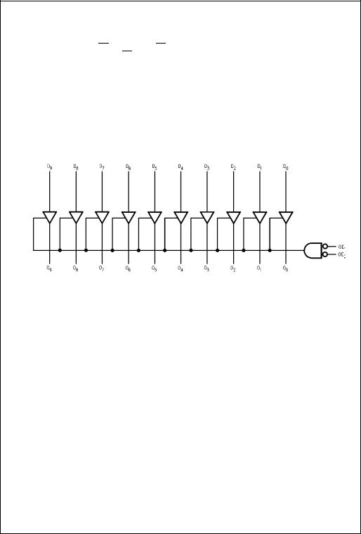
The ACTQ827 line driver is designed to be employed as memory address driver, clock driver and bus-oriented transmitter/receiver. The devices have 3-STATE outputs controlled by the Output Enable (OE) pins. When the OE is LOW, the device is transparent. When OE is HIGH, the device is in 3-STATE mode.
Function Table
|
Inputs |
Outputs |
Function |
||
|
|
|
|
|
|
|
|
|
Dn |
On |
|
|
OE |
|
|||
|
|
|
|
|
|
|
L |
|
H |
H |
Transparent |
|
L |
|
L |
L |
Transparent |
|
H |
|
X |
Z |
High Z |
|
|
|
|
|
|
H = HIGH Voltage Level
L = LOW Voltage Level
Z = HIGH Impedance
X = Immaterial
Logic Diagram
Please note that this diagram is provided only for the understanding of logic operations and should not be used to estimate propagation delays.
www.fairchildsemi.com |
2 |

Absolute Maximum Ratings(Note 1)
Supply Voltage (VCC) |
−0.5V to +7.0V |
DC Input Diode Current (IIK) |
|
VI = −0.5V |
−20 mA |
VI = VCC + 0.5V |
+20 mA |
DC Input Voltage (VI) |
−0.5V to VCC + 0.5V |
DC Output Diode Current (IOK) |
|
VO = −0.5V |
−20 mA |
VO = VCC + 0.5V |
+20 mA |
DC Output Voltage (VO) |
−0.5V to VCC + 0.5V |
DC Output Source |
|
or Sink Current (IO) |
± 50 mA |
DC VCC or Ground Current |
± 50 mA |
per Output Pin (ICC or IGND) |
|
Storage Temperature (TSTG) |
−65°C to +150°C |
DC Latch-Up Source |
|
or Sink Current |
± 300 mA |
Junction Temperature (TJ) |
140°C |
PDIP |
Recommended Operating
Conditions
Supply Voltage (VCC) |
4.5V to 5.5V |
Input Voltage (VI) |
0V to VCC |
Output Voltage (VO) |
0V to VCC |
Operating Temperature (TA) |
−40°C to +85°C |
Minimum Input Edge Rate V/ t |
125 mV/ns |
VIN from 0.8V to 2.0V |
|
VCC @ 4.5V, 5.5V |
|
Note 1: Absolute maximum ratings are those values beyond which damage to the device may occur. The databook specifications should be met, without exception, to ensure that the system design is reliable over its power supply, temperature, and output/input loading variables. Fairchild does not recommend operation of FACTä circuits outside databook specifications.
DC Electrical Characteristic
Symbol |
Parameter |
VCC |
TA = +25°C |
|
TA = −40°C to +85°C |
Units |
Conditions |
|
|
|
(V) |
Typ |
|
Guaranteed Limits |
|
|
|
|
|
|
|
|
|
|
|
|
VIH |
Minimum HIGH Level |
4.5 |
1.5 |
2.0 |
|
2.0 |
V |
VOUT = 0.1V |
|
Input Voltage |
5.5 |
1.5 |
2.0 |
|
2.0 |
|
or VCC − 0.1V |
VIL |
Maximum LOW Level |
4.5 |
1.5 |
0.8 |
|
0.8 |
V |
VOUT = 0.1V |
|
Input Voltage |
5.5 |
1.5 |
0.8 |
|
0.8 |
|
or VCC − 0.1V |
VOH |
Minimum HIGH Level |
4.5 |
4.49 |
4.4 |
|
4.4 |
V |
IOUT = −50 μA |
|
Output Voltage |
5.5 |
5.49 |
5.4 |
|
5.4 |
|
|
|
|
|
|
|
|
|
|
|
|
|
|
|
|
|
|
|
VIN = VIL or VIH |
|
|
4.5 |
|
3.86 |
|
3.76 |
V |
IOH = −24 mA |
|
|
5.5 |
|
4.86 |
|
4.76 |
|
IOH = −24 mA (Note 2) |
VOL |
Maximum LOW Level |
4.5 |
0.001 |
0.1 |
|
0.1 |
V |
IOUT = 50 μA |
|
Output Voltage |
5.5 |
0.001 |
0.1 |
|
0.1 |
|
|
|
|
|
|
|
|
|
|
|
|
|
|
|
|
|
|
|
VIN = VIL or VIH |
|
|
4.5 |
|
0.36 |
|
0.44 |
V |
IOL = 24 mA |
|
|
5.5 |
|
0.36 |
|
0.44 |
|
IOL = 24 mA (Note 2) |
IIN |
Maximum Input |
5.5 |
|
±0.1 |
|
±1.0 |
μA |
VI = VCC, GND |
|
Leakage Current |
|
|
|
|
|
|
|
|
|
|
|
|
|
|
|
|
IOZ |
Maximum 3-STATE |
5.5 |
|
±0.5 |
|
±5.0 |
μA |
VI = VIL, VIH |
|
Current |
|
|
|
|
|
|
VO = VCC, GND |
ICCT |
Maximum ICC/Input |
5.5 |
0.6 |
|
|
1.5 |
mA |
VI = VCC − 2.1V |
IOLD |
Minimum Dynamic |
5.5 |
|
|
|
75 |
mA |
VOLD = 1.65V Max |
IOHD |
Output Current (Note 3) |
5.5 |
|
|
|
−75 |
mA |
VOHD = 3.85V Min |
ICC |
Maximum Quiescent |
5.5 |
|
8.0 |
|
80.0 |
μA |
VIN = VCC |
|
Supply Current |
|
|
|
|
|
|
or GND |
|
|
|
|
|
|
|
|
|
VOLP |
Quiet Output |
5.0 |
1.1 |
1.6V |
|
|
V |
Figure 1, Figure 2 |
|
Maximum Dynamic VOL |
|
|
|
|
|
|
(Note 4)(Note 5) |
VOLV |
Quiet Output |
5.0 |
−0.6 |
−1.3 |
|
|
V |
Figure 1, Figure 2 |
|
Minimum Dynamic VOL |
|
|
|
|
|
|
(Note 4)(Note 5) |
VIHD |
Minimum HIGH Level |
5.0 |
1.9 |
2.0 |
|
|
V |
(Note 4)(Note 6) |
|
Dynamic Input Voltage |
|
|
|
|
|
|
|
|
|
|
|
|
|
|
|
|
VILD |
Maximum LOW Level |
5.0 |
1.2 |
0.8 |
|
|
V |
(Note 4)(Note 6) |
|
Dynamic Input Voltage |
|
|
|
|
|
|
|
|
|
|
|
|
|
|
|
|
74ACTQ827
3 |
www.fairchildsemi.com |
 Loading...