


Fairchild Semiconductor 74ACTQ18823SSCX, 74ACTQ18823SSC, 74ACTQ18823MTDX, 74ACTQ18823MTD, 74ACTQ18823CW Datasheet
September 1991
Revised November 1999
74ACTQ18823
18-Bit D-Type Flip-Flop with 3-STATE Outputs
General Description
The ACTQ18823 contains eighteen non-inverting D-type flip-flops with 3-STATE outputs and is intended for bus oriented applications. The device is byte controlled. A buffered clock (CP), Clear (CLR), Clock Enable (EN) and Output Enable (OE) are common to each byte and can be shorted together for full 18-bit operation.
The ACTQ18823 utilizes Fairchild’s Quiet Series technology to guarantee quiet output switching and improved dynamic threshold performance. FACT Quiet Series features GTO output control and undershoot corrector for superior performance.
Features
■Utilizes Fairchild’s FACT Quiet Series technology
■Broadside pinout allows for easy board layout
■Guaranteed simultaneous switching noise level and dynamic threshold performance
■Guaranteed pin-to-pin output skew
■Separate control logic for each byte
■Extra data width for wider address/data paths or buses carrying parity
■Outputs source/sink 24 mA
■Additional specs for Multiple Output Switching
■Output loading specs for both 50 pF and 250 pF loads
Ordering Code:
Order Number |
Package Number |
Package Description |
|
|
|
74ACTQ18823SSC |
MS56A |
56-Lead Shrink Small Outline Package (SSOP), JEDEC MO-118, 0.300” Wide |
|
|
|
74ACTQ18823MTD |
MTD56 |
56-Lead Thin Shrink Small Outline Package (TSSOP), JEDEC MO-153, 6.1mm Wide |
|
|
|
Device also available in Tape and Reel. Specify by appending suffix letter “X” to the ordering code.
Logic Symbol
Pin Descriptions
|
|
Pin Names |
Description |
|||
|
|
|
|
|
||
|
|
|
|
n |
Output Enable Input (Active LOW) |
|
|
|
OE |
||||
|
|
|
Clear (Active LOW) |
|||
|
CLR |
n |
||||
|
|
Clock Enable (Active LOW) |
||||
|
EN |
n |
||||
|
CPn |
Clock Pulse Input |
||||
|
I0–I17 |
Inputs |
||||
|
O0–O17 |
Outputs |
||||
FACT |
, Quiet Series |
, FACT Quiet Series |
, and GTO are trademarks of Fairchild Semiconductor Corporation. |
Outputs STATE-3 with Flop-Flip Type-D Bit-18 74ACTQ18823
© 1999 Fairchild Semiconductor Corporation |
DS010953 |
www.fairchildsemi.com |
74ACTQ18823
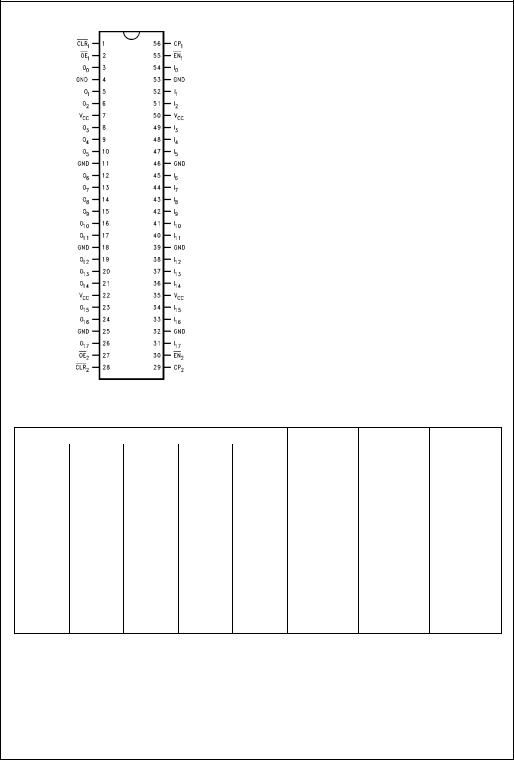
Connection Diagram |
Functional Description |
||||||||||||||||||
|
The ACTQ18823 consists of eighteen D-type edge-trig- |
||||||||||||||||||
|
gered flip-flops. These have 3-STATE outputs for bus sys- |
||||||||||||||||||
|
tems organized with inputs and outputs on opposite sides. |
||||||||||||||||||
|
The device is byte controlled with each byte functioning |
||||||||||||||||||
|
identically, but independent of the other. The control pins |
||||||||||||||||||
|
can be shorted together to obtain full 16-bit operation. The |
||||||||||||||||||
|
following description applies to each byte. The buffered |
||||||||||||||||||
|
clock (CPn) and buffered Output Enable |
(OE |
n) are com- |
||||||||||||||||
|
mon to all flip-flops within that byte. The flip-flops will store |
||||||||||||||||||
|
the state of their individual D inputs that meet set-up and |
||||||||||||||||||
|
hold time requirements on the LOW-to-HIGH CPn transi- |
||||||||||||||||||
|
tion. With |
OE |
n LOW, the contents of the flip-flops are avail- |
||||||||||||||||
|
able at the outputs. When |
OE |
n is HIGH, the outputs go to |
||||||||||||||||
|
the impedance state. Operation of the |
OE |
n input does not |
||||||||||||||||
|
affect the state of the flip-flops. In addition to the Clock and |
||||||||||||||||||
|
Output Enable pins, there are Clear (CLRn) and Clock |
||||||||||||||||||
|
Enable |
(EN |
n) pins. These devices are ideal for parity bus |
||||||||||||||||
|
interfacing in high performance systems. |
||||||||||||||||||
|
|
|
|
|
|
|
|
||||||||||||
|
When |
CLR |
n is LOW and |
OE |
n is LOW, the outputs are |
||||||||||||||
|
LOW. When |
CLR |
n is HIGH, data can be entered into the |
||||||||||||||||
|
flip-flops. When |
EN |
n is LOW, data on the inputs is trans- |
||||||||||||||||
|
ferred to the outputs on the LOW-to-HIGH clock transition. |
||||||||||||||||||
|
When the ENn is HIGH, the outputs do not change state, |
||||||||||||||||||
|
regardless of the data or clock input transitions. |
||||||||||||||||||
Function Table (Note 1)
|
|
|
|
Inputs |
|
|
Internal |
Output |
Function |
||
|
|
|
|
|
|
|
|
|
|
|
|
OE |
|
CLR |
|
EN |
CP |
In |
Q |
On |
|||
|
|
|
|||||||||
|
H |
|
X |
|
L |
|
L |
L |
Z |
High Z |
|
|
H |
|
X |
|
L |
|
H |
H |
Z |
High Z |
|
|
H |
|
L |
|
X |
X |
X |
L |
Z |
Clear |
|
|
L |
|
L |
|
X |
X |
X |
L |
L |
Clear |
|
|
H |
|
H |
|
H |
X |
X |
NC |
Z |
Hold |
|
|
L |
|
H |
|
H |
X |
X |
NC |
NC |
Hold |
|
|
H |
|
H |
|
L |
|
L |
L |
Z |
Load |
|
|
H |
|
H |
|
L |
|
H |
H |
Z |
Load |
|
|
L |
|
H |
|
L |
|
L |
L |
L |
Load |
|
|
L |
|
H |
|
L |
|
H |
H |
H |
Load |
|
H= HIGH Voltage Level
L= LOW Voltage Level
X= Immaterial
Z= High Impedance
= LOW-to-HIGH Transition
NC= No Change
Note 1: The table represents the logic for one byte. The two bytes are independent of each other and function identically.
www.fairchildsemi.com |
2 |

Logic Diagrams
Byte 1 (0:8)
Byte 2 (9:17)
74ACTQ18823
3 |
www.fairchildsemi.com |
 Loading...