


Fairchild Semiconductor 74F112SJX, 74F112SJ, 74F112SCX, 74F112SC, 74F112PC Datasheet
...
April 1988
Revised July 1999
74F112
Dual JK Negative Edge-Triggered Flip-Flop
General Description
The 74F112 contains two independent, high-speed JK flipflops with Direct Set and Clear inputs. Synchronous state changes are initiated by the falling edge of the clock. Triggering occurs at a voltage level of the clock and is not directly related to the transition time. The J and K inputs can change when the clock is in either state without affecting the flip-flop, provided that they are in the desired state during the recommended setup and hold times relative to the falling edge of the clock. A LOW signal on SD or CD
prevents clocking and forces Q or Q HIGH, respectively.
Simultaneous LOW signals on SD and CD force both Q and
Q HIGH.
Asynchronous Inputs:
LOW input to SD sets Q to HIGH level
LOW input to CD sets Q to LOW level
Clear and Set are independent of clock
Simultaneous LOW on CD and SD makes both Q
and Q HIGH
Ordering Code:
Order Number |
Package Number |
Package Description |
|
|
|
74F112SC |
M16A |
16-Lead Small Outline Integrated Circuit (SOIC), JEDEC MS-012, 0.150 Narrow |
|
|
|
74F112SJ |
M16D |
16-Lead Small Outline Package (SOP), EIAJ TYPE II, 5.3mm Wide |
|
|
|
74F112PC |
N16E |
16-Lead Plastic Dual-In-Line Package (PDIP), JEDEC MS-001, 0.300 Wide |
|
|
|
Devices also available in Tape and Reel. Specify by appending the suffix letter “X” to the ordering code.
Logic Symbols |
Connection Diagram |
IEEE/IEC
Flop-Flip Triggered-Edge Negative JK Dual 74F112
© 1999 Fairchild Semiconductor Corporation |
DS009472 |
www.fairchildsemi.com |
74F112
Unit Loading/Fan Out
|
|
|
|
Pin Names |
|
|
|
|
|
|
Description |
|
|
|
|
|
U.L. |
|
|
|
|
Input IIH/IIL |
||||||||||||||
|
|
|
|
|
|
|
|
|
|
|
|
|
HIGH/LOW |
Output IOH/IOL |
||||||||||||||||||||||
|
|
|
|
|
|
|
|
|
|
|
|
|
|
|
|
|
|
|
|
|
|
|
|
|
|
|
|
|||||||||
|
|
|
|
|
|
|
|
|
|
|
|
|
|
|
|
|
|
|
|
|
|
|
||||||||||||||
|
|
J1, J2, K1, K2 |
|
Data Inputs |
|
|
|
|
|
1.0/1.0 |
|
|
|
20 μA/−0.6 mA |
||||||||||||||||||||||
|
|
|
|
|
|
|
|
|
|
|
2 |
|
|
|
|
Clock Pulse Inputs (Active Falling Edge) |
1.0/4.0 |
|
|
|
20 μA/−2.4 mA |
|||||||||||||||
|
|
CP |
1, |
|
|
CP |
|
|
|
|
|
|
|
|||||||||||||||||||||||
|
|
|
|
|
|
|
D2 |
|
Direct Clear Inputs (Active LOW) |
|
1.0/5.0 |
|
|
|
20 μA/−3.0 mA |
|||||||||||||||||||||
|
|
C |
D1, |
C |
|
|
|
|
|
|||||||||||||||||||||||||||
|
|
|
|
D2 |
|
Direct Set Inputs (Active LOW) |
|
1.0/5.0 |
|
|
|
20 μA/−3.0 mA |
||||||||||||||||||||||||
|
|
S |
D1, |
S |
|
|
|
|
|
|||||||||||||||||||||||||||
|
|
|
|
|
|
|
|
|
|
|
|
|
|
|
|
|
|
|
|
|
|
−1 mA/20 mA |
||||||||||||||
|
|
Q1, Q2, |
Q |
1, |
Q |
2 |
Outputs |
|
|
|
|
|
|
|
50/33.3 |
|
|
|||||||||||||||||||
Truth Table |
|
|
|
|
|
|
|
|
|
|
|
|
|
|
|
|
|
|
|
|
|
|||||||||||||||
|
|
|
|
|
|
|
|
|
|
|
|
|
|
|
|
|
|
|
|
|
|
|
|
|
|
|
|
|
||||||||
|
|
|
|
|
|
|
|
|
|
|
|
|
|
|
|
|
|
|
|
|
|
Inputs |
|
|
|
Outputs |
|
|
||||||||
|
|
|
|
|
|
|
|
|
|
|
|
|
|
|
|
|
|
|
|
|
|
|
|
|
|
|
|
|
|
|
|
|
|
|
|
|
|
|
|
|
|
|
|
|
|
|
|
|
|
|
|
|
|
|
|
|
|
|
|
|
|
|
|
|
|
|
|
|
|
|
|
|
|
|
|
|
|
|
|
|
|
|
|
|
|
|
|
|
|
|
|
SD |
CD |
CP |
J |
K |
|
Q |
|
|
Q |
|
|
|||||||
|
|
|
|
|
|
|
|
|
|
|
|
|
|
|
|
|
|
L |
H |
|
X |
X |
X |
|
H |
|
|
L |
|
|
||||||
|
|
|
|
|
|
|
|
|
|
|
|
|
|
|
|
|
|
H |
L |
|
X |
X |
X |
|
L |
|
|
H |
|
|
||||||
|
|
|
|
|
|
|
|
|
|
|
|
|
|
|
|
|
|
L |
L |
|
X |
X |
X |
|
H |
|
|
H |
|
|
||||||
|
|
|
|
|
|
|
|
|
|
|
|
|
|
|
|
|
|
H |
H |
|
|
h |
h |
|
Q0 |
|
|
|||||||||
|
|
|
|
|
|
|
|
|
|
|
|
|
|
|
|
|
|
|
|
|
Q |
0 |
|
|
||||||||||||
|
|
|
|
|
|
|
|
|
|
|
|
|
|
|
|
|
|
H |
H |
|
|
l |
h |
|
L |
|
|
H |
|
|
||||||
|
|
|
|
|
|
|
|
|
|
|
|
|
|
|
|
|
|
H |
H |
|
|
h |
l |
|
H |
|
|
L |
|
|
||||||
|
|
|
|
|
|
|
|
|
|
|
|
|
|
|
|
|
|
H |
H |
|
|
|
|
|
|
|
|
|
|
|
||||||
|
|
|
|
|
|
|
|
|
|
|
|
|
|
|
|
|
|
|
|
l |
l |
|
Q0 |
Q0 |
|
|
||||||||||
H (h) = HIGH Voltage Level
L (l) = LOW Voltage Level X = Immaterial
= HIGH-to-LOW Clock Transition
Q0(Q0) = Before HIGH-to-LOW Transition of Clock
Lower case letters indicate the state of the referenced input or output one setup time prior to the HIGH-to-LOW clock transition.
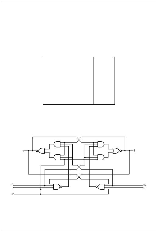
Logic Diagram
(One Half Shown)
Please note that this diagram is provided only for the understanding of logic operations and should not be used to estimate propagation delays.
www.fairchildsemi.com |
2 |
 Loading...