


74ACTQ240SJ
Fairchild Semiconductor 74ACTQ240SJ, 74ACTQ240SCX, 74ACTQ240SC, 74ACTQ240QSCX, 74ACTQ240QSC Datasheet
...
© 1999 Fairchild Semiconductor Corporation DS010234 www.fairchildsemi.com
July 1989
Revised November 1999
74ACQ240 • 74ACTQ240 Quiet Series Octal Buffer/Line Driver with 3-STATE Outputs
74ACQ240 • 74ACTQ240
Quiet Series Octal Buffer/Line Driver
with 3-STA TE Outputs
General Description
The ACQ/ACTQ240 is an inverting octal buffer and line
driver designed to be employed as a memory address
driver, clock driver and bus oriented tr ansmitt er or r eceiv er
which provides improved PC board density. The ACQ/
ACTQ utilizes Fairchild’s Quiet Series technology to
guarantee quiet output switching and improve dynamic
threshold performance. FACT Quiet Series features
GTO output control and unde rshoot corre ctor in add ition
to a split ground bus for superior performance.
Features
■ ICC and IOZ reduced by 5 0%
■ Guaranteed simultaneous switching noise level and
dynamic threshold performan ce
■ Guarante ed pin-to-pin skew AC performance
■ Improved latch-up immunity
■ Inverting 3-STATE outputs drive bus lines or buffer
memory address registers
■ Outputs source/sink 24 mA
■ Faster prop delays than the standard ACT240
Ordering Code:
Device also available in Tape and Reel. Specify by appending suffix letter “X” to the ordering code.
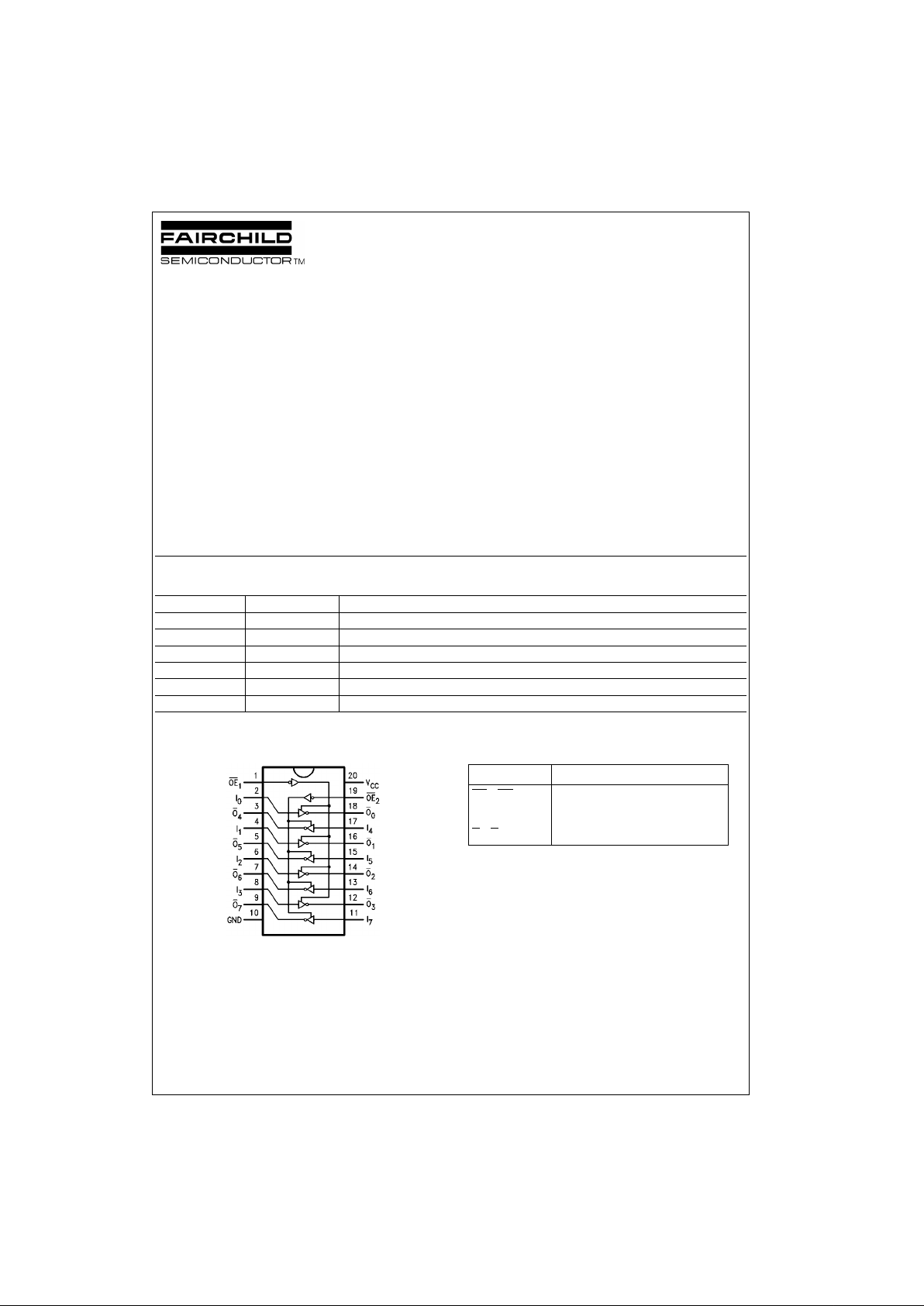
Connection Diagram Pin Descriptions
FACT, Qui et Series , FACT Quiet Series, an d GTO are trademarks of Fairchild Semiconductor Corporation.
Order Number Package Number Package Description
74ACQ240SC M20B 20-Lead Small Outline Integrated Circuit (SOIC)JEDEC MS-013, 0.300” Wide Body
74ACQ240SJ M20D 20-Lead Small Outline Package (SOP), EIAJ TYPE II, 5.3mm Wide
74ACQ240PC N20A 20-Lead Plastic Dual-In-Line Package (PDIP), JEDEC MS-001, 0.300” Wide
74ACTQ240SC M20B 20-Lead Small Outline Integrated Circuit (SOIC)JEDEC MS-013, 0.300” Wide Body
74ACTQ240SJ M20D 20-Lead Small Outline Package (SOP), EIAJ TYPE II, 5.3mm Wide
74ACTQ240QSC MQA20 20-Lead Quarter Size Outline Package (QSOP), JEDEC MO-137, 0.150” Wide
Pin Names Description
OE
1
, OE
2
3-STATE Output Enable Inputs
I
0–I7
Inputs
O
0–O7
Outputs
www.fairchildsemi.com 2
74ACQ240 • 74ACTQ240
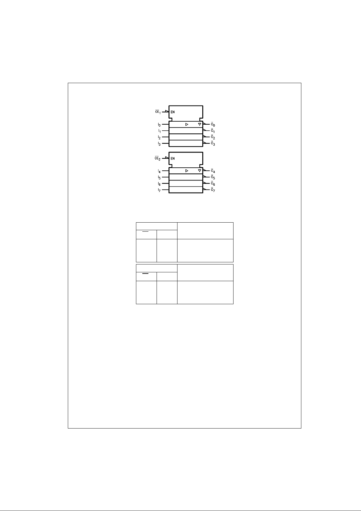
Logic Symbol
IEEE/IEC
Truth Tables
H = HIGH Voltage Level
L = LOW Voltage Level
X = Immaterial
Z = High Impedance
Inputs Outputs
OE
1
I
n
(Pins 12, 14, 16, 18)
LL H
LH L
HX Z
Inputs Outputs
OE
2
I
n
(Pins 3, 5, 7, 9)
L L H
LH L
HX Z
3 www.fairchildsemi.com
74ACQ240 • 74ACTQ240
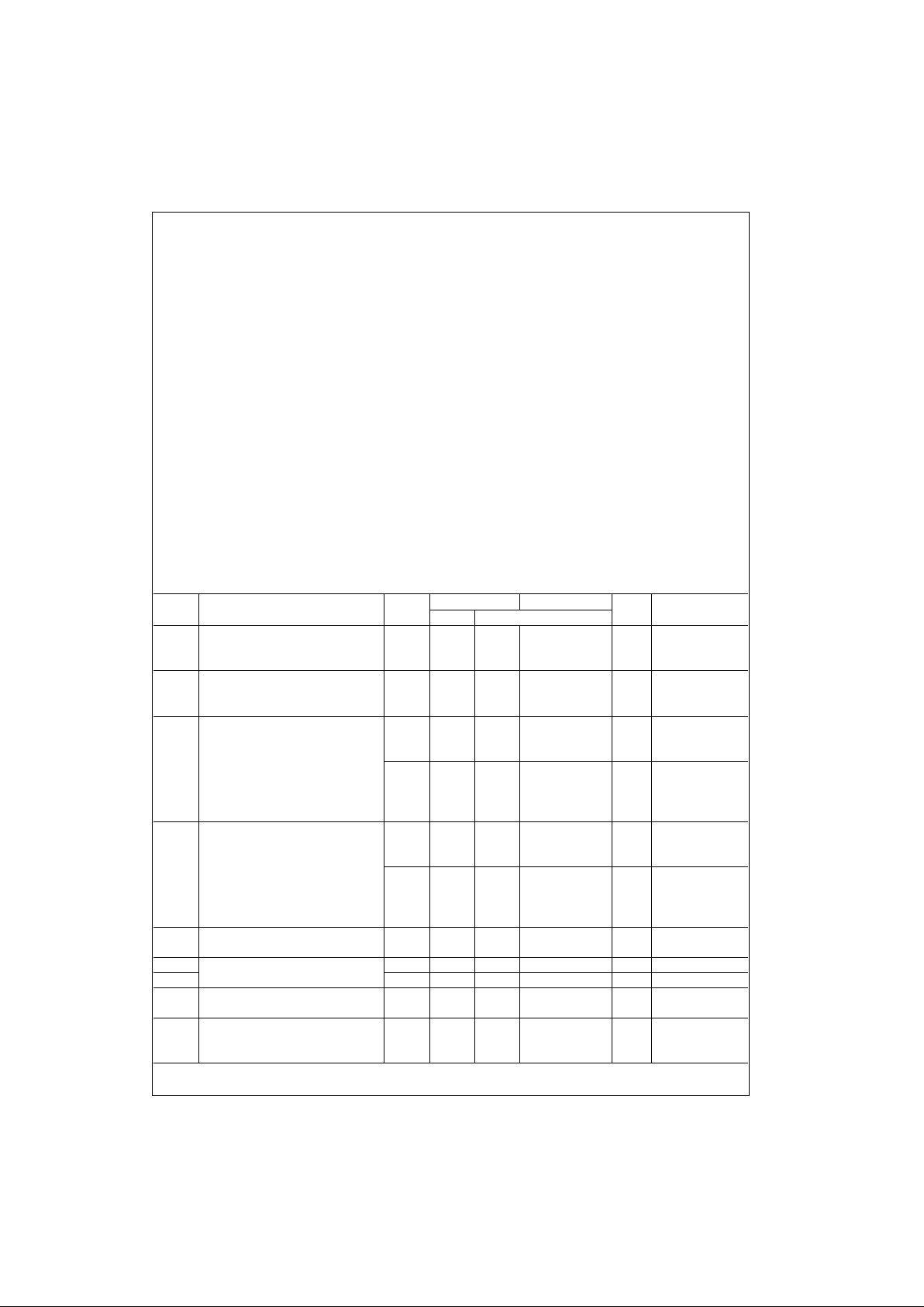
Absolute Maximum Ratings(Note 1) Recommended Operating
Conditions
Note 1: Absolute max imum rating s are those va lues beyon d w hich damage
to the device may occu r. The databook spe cificatio ns shou ld be met, wit hout exception, to ensure that the system de sign is relia ble over its p ower
supply, temperature, and output/input loading variables. Fairchild does not
recommend operation of FACT circuits outside databook specificat ions.
DC Electrical Characteristics for ACQ
Supply Voltage (VCC) −0.5V to +7.0V
DC Input Diode Current (I
IK
)
V
I
= −0.5V −20 mA
V
I
= VCC + 0.5V +20 mA
DC Input Voltage (V
I
) −0.5V to VCC + 0.5V
DC Output Diode Current (I
OK
)
V
O
= −0.5V −20 mA
V
O
= VCC + 0.5V +20 mA
DC Output Voltage (V
O
) −0.5V to VCC + 0.5V
DC Output S ource
or Sink Current (I
O
) ±50 mA
DC V
CC
or Ground Current
per Output Pin (I
CC
or I
GND
) ±50 mA
Storage Temperature (T
STG
) −65°C to +150°C
DC Latch-Up Source or
Sink Current ±300 mA
Junction Temperature (T
J
)
PDIP 140°C
Supply Voltage (V
CC
)
ACQ 2.0V to 6.0V
ACTQ 4.5V to 5.5V
Input Voltage (V
I
)0V to V
CC
Output Voltage (VO)0V to V
CC
Operating Temperature (TA) −40°C to +85°C
Minimum Input Edge Rate ∆V/∆t
ACQ Devices
V
IN
from 30% to 70% of V
CC
VCC @ 3.0V, 4.5V, 5.5V 125 mV/ns
Minimum Input Edge Rate ∆V/∆t
ACTQ Devices
V
IN
from 0.8V to 2.0V
V
CC
@ 4.5V, 5.5V 125 mV/ns
Symbol Parameter
V
CC
TA = +25°C TA = −40°C to +85°C
Units Conditions
(V) Typ Guaranteed Limits
V
IH
Minimum HIGH Level 3.0 1.5 2.1 2.1 V
OUT
= 0.1V
Input Voltage 4.5 2.25 3.15 3.15 V or VCC − 0.1V
5.5 2.75 3.85 3.85
V
IL
Maximum LOW Level 3.0 1.5 0.9 0.9 V
OUT
= 0.1V
Input Voltage 4.5 2.25 1.35 1.35 V or VCC − 0.1V
5.5 2.75 1.65 1.65
V
OH
Minimum HIGH Level 3.0 2.99 2.9 2.9
Output Voltage 4.5 4.49 4.4 4.4 V I
OUT
= −50 µA
5.55.495.4 5.4
VIN = V
IL
or V
IH
3.0 2.56 2.46 IOH = −12 mA
4.5 3.86 3.76 V I
OH
= −24 mA
5.5 4.86 4.76 I
OH
= −24 mA (Note 2)
V
OL
Maximum LOW Level 3.0 0.002 0.1 0.1
Output Voltage 4.5 0.001 0.1 0.1 V I
OUT
= 50 µA
5.5 0.001 0.1 0.1
VIN = VIL or V
IH
3.0 0.36 0.44 IOL = 12 mA
4.5 0.36 0.44 V IOL = 24 mA
5.5 0.36 0.44 IOL = 24 mA (Note 2)
I
IN
Maximum Input
5.5 ±0.1 ±1.0 µAVI = VCC, GND
(Note 4) Leakage Current
I
OLD
Minimum Dynamic 5.5 75 mA V
OLD
= 1.65V Max
I
OHD
Output Current (Note3) 5.5 −75 mA V
OHD
= 3.85V Min
I
CC
Maximum Quiescent
5.5 4.0 40.0 µAVIN = VCC or GND
(Note 4) Supply Current
I
OZ
Maximum 3-STATE
5.5 ±0.25 ±2.5 µA
VI (OE) = VIL, V
IH
Leakage Current VI = VCC, GND
VO = VCC, GND
 Loading...