


74ACTQ821CW
March 1990
Revised November 1998
74ACTQ821 Quiet Series 10-Bit D-Type Flip-Flop with 3-STATE Outputs
© 1999 Fairchild Semiconductor Corporation DS010686.prf www.fairchildsemi.com
74ACTQ821
Quiet Series 10-Bit D-Type Flip-Flop
with 3-STATE Outputs
General Description
The ACTQ821 is a 10-bit D-type flip-f lop with no n-invert ing
3-STATE outputs arranged in a broadside pinout. The
ACTQ821 utilizes Fairchild’s Quiet Series technology to
guarantee quiet output switching and improved dynamic
threshold performance. FACT Quiet Series features
GTO output control and und ershoot c orrector in a ddition
to a split ground bus for superior performance.
Features
■ Guaranteed simultaneous switching noise level and
dynamic threshold performance
■ Guaranteed pin-to-pin skew AC performance
■ Non-inverting 3-STATE outputs for bus interfacing
■ 4 kV minimum ESD immunity
■ Outputs source/sink 24 mA
■ Functionally identical to the AM29821
Ordering Code:
Device also available in Tape and Reel. Specify by appendin g s uf f ix let t er “X” to the ordering co de.
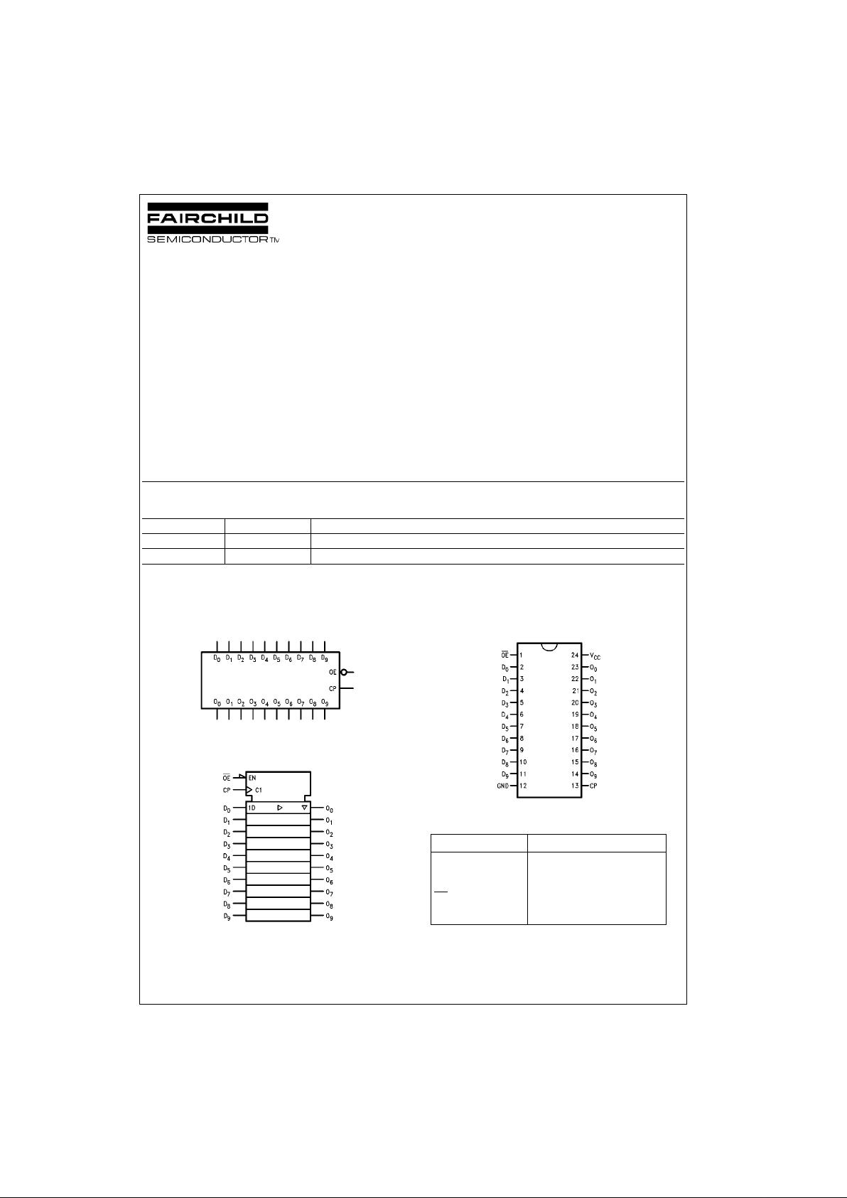
Logic Symbols
IEEE/IEC
Connection Diagram
Pin Assignment
for DIP and SOIC
Pin Descriptions
FACT, Quiet Series, FACT Quiet Series, and GTO are trademark s of Fairchild Semiconductor Corporation.
Order Number Package Number Package Description
74ACTQ821SC M24B 24-Lead Small Outline Integrated Circuit (SOIC), JEDEC MS-013, 0.300” Wide Body
74ACTQ821SPC N24C 24-Lead Plastic Dual-In-Line Package (PDIP), JEDEC MS-100, 0.300” Wide
Pin Names Description
D
0–D9
Data Inputs
O
0–O9
Data Outp uts
OE
Output Enable Input
CP Clock Input
www.fairchildsemi.com 2
74ACTQ821
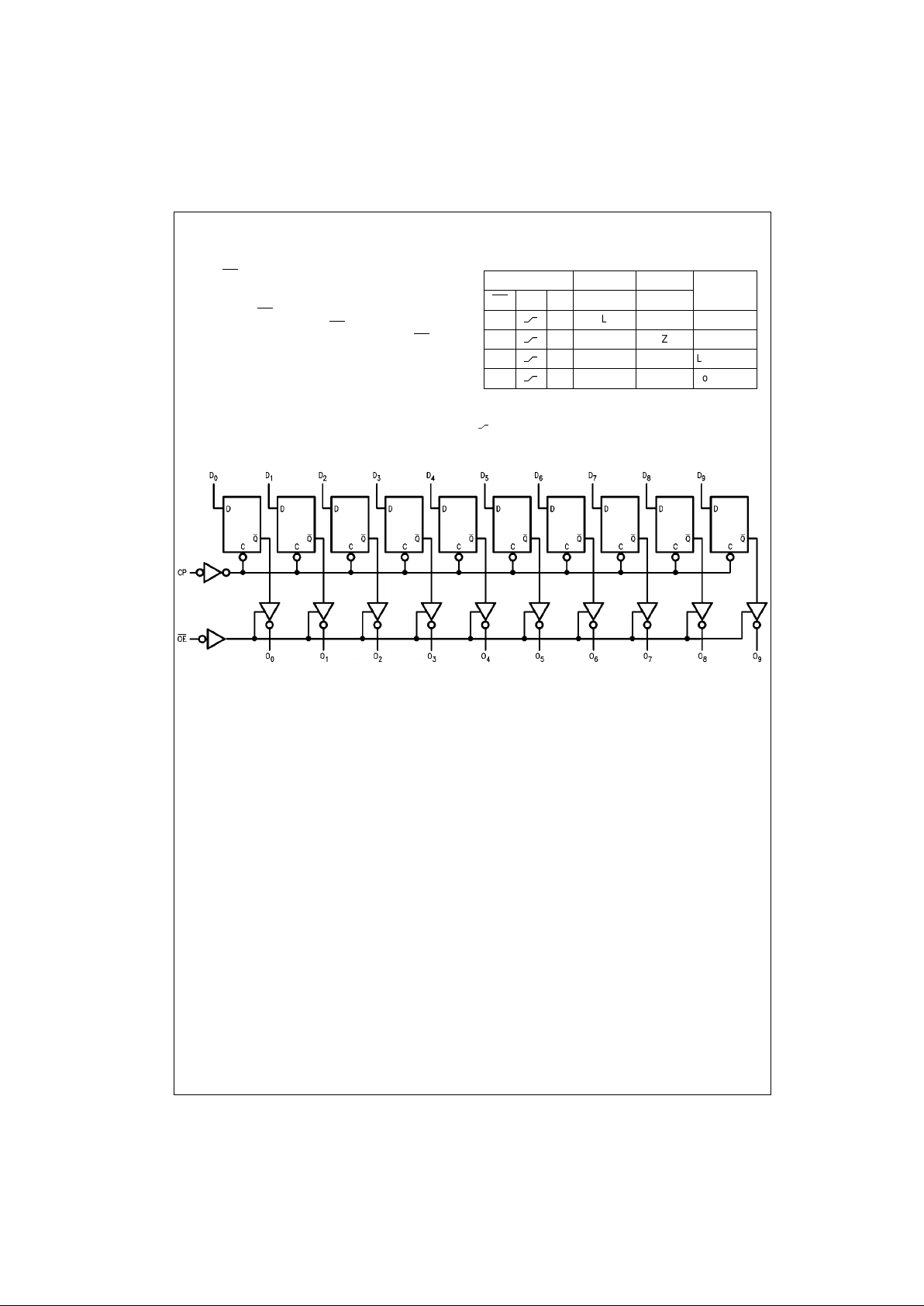
Functional Description
The ACTQ821 consists of ten-bit D-type edge-triggered
flip-flops. The buffered Clock (CP) and buffered Output
Enable (OE
) are common to all flip-flops. The flip-flops will
store the state of the ir individual D inputs that meet the
setup and hold time requirements on the LOW-to-HIGH CP
transition. With OE
LOW the contents of the flip-flops are
available at the outputs. When OE
is HIGH the outputs go
to the high impedance state. Operation of the OE
input
does not affect the state of the flip-flops.
The ACTQ821 is function ally and pin compatible wit h the
AM29821.
Function Table
H = HIGH Voltage Level
L = LOW Voltage Level
Z = HIGH Impedance
= LOW-to-HIGH Clock Transition
Logic Diagram
Please note that this diagram is provided only for the understanding of logic operations and should not be used to estimate p ropagation delays.
Inputs Internal Outputs Function
OE
CP D Q O
H
L L Z High Z
H
H H Z High Z
L
LL LLoad
L
HH HLoad
3 www.fairchildsemi.com
74ACTQ821
Absolute Maximum Ratings(Note 1)
Recommended Operating
Conditions
Note 1: Absolute maximum ratings are those values beyond which damage
to the device may occur. The databook specifications should be met, without exception, to ensure that the system design is reliable over its power
supply, temperature, and output/in put loading variables. Fairchild does n ot
recommend operat ion of FACT circuits outside databook specifications.
DC Electrical Characteristics
Note 2: All outputs loaded; thresholds on input associated with output under test.
Note 3: Maximum test duration 2.0 ms, one output loaded at a time.
Note 4: DIP package.
Note 5: Max number of ou t puts defined as (n). Data inputs are driven 0V to 3V. One output @ GND.
Supply Voltage (VCC) − 0.5V to + 7.0V
DC Input Diode Current (I
IK
)
V
I
= − 0.5V − 20 mA
V
I
= VCC + 0.5V + 20 mA
DC Input Voltage (V
I
) − 0.5V to VCC + 0.5V
DC Output Diode Current (I
OK
)
V
O
= − 0.5V − 20 mA
V
O
= VCC + 0.5V + 20 mA
DC Output Voltage (V
O
) − 0.5V to VCC + 0.5V
DC Output Source
or Sink Current (I
O
) ± 50 mA
DC V
CC
or Ground Current
per Output Pin (I
CC
or I
GND
) ± 50 mA
Storage Temperature (T
STG
) − 65°C to + 150°C
DC Latch-Up Source
or Sink Current ± 300 mA
Junction Temperature (T
J
)
PDIP 140°C
Supply Voltage (V
CC
) 4.5V to 5.5V
Input Voltage (V
I
)0V to V
CC
Output Voltage (VO)0V to V
CC
Operating Temperature (TA) − 40°C to + 85°C
Minimum Input Edge Rate ∆V/∆t
Minimum Input Edge Rate ∆V/∆t 125 mV/ns
V
IN
from 0.8V to 2.0V
V
CC
@ 4.5V, 5.5V
Symbol Parameter
V
CC
TA = + 25°CTA = − 40°C to + 85°C
Units Conditions
(V) Typ Guaranteed Limits
V
IH
Minimum High Level 4.5 1.5 2.0 2.0 V V
OUT
= 0.1V
Input Voltage 5.5 1.5 2.0 2.0 or VCC − 0.1V
V
IL
Maximum Low Level 4.5 1.5 0.8 0.8 V V
OUT
= 0.1V
Input Voltage 5.5 1.5 0.8 0.8 or VCC − 0.1V
V
OH
Minimum High Level 4.5 4.49 4.4 4.4 V I
OUT
= − 50 µA
Output Voltage 5.5 5.49 5.4 5.4
VIN = VIL or V
IH
4.5 3.86 3.76 V IOH = − 24 mA
5.5 4.86 4.76 IOH = − 24 mA (Note 2)
V
OL
Maximum Low Level 4.5 0.001 0.1 0.1 V I
OUT
= 50 µA
Output Voltage 5.5 0.001 0.1 0.1
VIN = VIL or V
IH
4.5 0.36 0.44 V IOL = 24 mA
5.5 0.36 0.44 IOL = 24 mA (Note 2)
I
IN
Maximum Input Leakage Current 5.5 ±0.1 ±1.0 µAVI = VCC, GND
I
OZ
Maximum 3- STATE 5.5 ±0.5 ±5.0 µAVI = VIL, V
IH
Leakage Current VO = VCC, GND
I
CCT
Maximum ICC/Input 5.5 0.6 1.5 mA VI = VCC − 2.1V
I
OLD
Minimum Dynamic 5.5 75 mA V
OLD
= 1.65V Max
I
OHD
Output Current (Note 3) 5.5 −75 mA V
OHD
= 3.85V Min
I
CC
Maximum Quiescent Supply Current 5.5 8.0 80.0 µAVIN = VCC or GND
V
OLP
Quiet Output
Maximum Dynamic V
OL
5.0 1.1 1.5 V Figure 1, Figure 2
(Note 4)(Note 5)
V
OLV
Quiet Output
Minimum Dynamic V
OL
5.0 − 0.6 − 1.2 V Figure 1, Figure 2
(Note 4)(Note 5)
V
IHD
Minimum High Level
Dynamic Input Voltage
5.0 1.9 2.2 V (Note 4)(Note 6)
V
ILD
Maximum Low Level
Dynamic Input Voltage
5.0 1.2 0.8 V (Note 4)(Note 6)
 Loading...