


April 1988
Revised November 1999
74F109
Dual JK Positive Edge-Triggered Flip-Flop
General Description |
Asynchronous Inputs: |
||||||||
The F109 consists of two high-speed, completely indepen- |
LOW input to |
S |
D sets Q to HIGH level |
||||||
dent transition clocked JK flip-flops. The clocking operation |
LOW input to |
C |
D sets Q to LOW level |
||||||
is independent of rise and fall times of the clock waveform. |
Clear and Set are independent of clock |
||||||||
The JK design allows operation as a D-type flip-flop (refer |
|||||||||
|
|
|
|
|
|
|
|
||
Simultaneous LOW on CD and SD makes |
|||||||||
to F74 data sheet) by connecting the J and K inputs. |
|||||||||
|
|
|
|
|
|
|
|
||
both Q and Q HIGH |
|||||||||
|
|||||||||
Ordering Code:
Order Number |
Package Number |
Package Description |
|
|
|
74F109SC |
M16A |
16-Lead Small Outline Integrated Circuit (SOIC), JEDEC MS-012, 0.150” Narrow Body |
|
|
|
74F109SJ |
M16D |
16-Lead Small Outline Package (SOP), EIAJ TYPE 11, 5.3mm Wide |
|
|
|
74F109PC |
N16E |
16-Lead Plastic Dual-In-Line Package (PDIP), JEDEC MS-001, 0.300” Wide |
|
|
|
Devices also available in Tape and Reel. Specify by appending suffix letter “X” to the ordering code.
Logic Symbols |
Connection Diagram |
IEEE/IEC
Flop-Flip Triggered-Edge Positive JK Dual 74F109
© 1999 Fairchild Semiconductor Corporation |
DS009471 |
www.fairchildsemi.com |
74F109
Truth Table
|
|
|
|
|
Inputs |
|
|
|
|
Outputs |
||
|
|
|
|
|
|
|
|
|
|
|
|
|
|
SD |
CD |
|
|
|
|
|
|
|
|
||
|
CP |
J |
K |
|
Q |
|
Q |
|||||
|
L |
H |
X |
X |
X |
|
H |
|
L |
|||
|
H |
L |
X |
X |
X |
|
L |
|
H |
|||
|
L |
L |
X |
X |
X |
|
H |
|
H |
|||
|
H |
H |
|
I |
I |
|
L |
|
H |
|||
|
H |
H |
|
h |
I |
|
|
Toggle |
||||
|
H |
H |
|
I |
h |
|
Q |
|
|
|||
|
|
|
|
Q |
|
|||||||
|
H |
H |
|
h |
h |
|
H |
|
L |
|||
|
H |
H |
L |
X |
X |
|
Q |
|
|
|||
|
|
|
Q |
|
||||||||
H (h) = |
HIGH Voltage Level |
L (l) = |
LOW Voltage Level |
= |
LOW-to-HIGH Transition |
X = |
Immaterial |
Q0 (Q0) = Before LOW-to-HIGH Transition of Clock
Lower case letters indicate the state of the referenced output one setup time prior to the LOW-to-HIGH clock transition.
Unit Loading/Fan Out
|
|
|
Pin Names |
Description |
U.L. |
Input IIH/IIL |
|||||||||||
|
|
|
HIGH/LOW |
Output IOH/IOL |
|||||||||||||
|
|
|
|
|
|
|
|
|
|
|
|
|
|
|
|
||
|
|
|
|
|
|
|
|
|
|
|
|
|
|
|
|
||
|
J1, J2, |
|
|
|
1, |
|
2 |
|
Data Inputs |
1.0/1.0 |
20 µ A/− 0.6 mA |
||||||
|
K |
K |
|
||||||||||||||
|
CP1, CP2 |
Clock Pulse Inputs (Active Rising Edge) |
1.0/1.0 |
20 µ A/− 0.6 mA |
|||||||||||||
|
|
|
|
|
|
D2 |
Direct Clear Inputs (Active LOW) |
1.0/3.0 |
20 µ A/− 1.8 mA |
||||||||
|
C |
D1, |
C |
||||||||||||||
|
|
|
D2 |
Direct Set Inputs (Active LOW) |
1.0/3.0 |
20 µ A/− 1.8 mA |
|||||||||||
|
S |
D1, |
S |
||||||||||||||
|
|
|
|
|
− 1 mA/20 mA |
||||||||||||
|
Q1, Q2, |
Q |
1, |
Q |
2 |
Outputs |
50/33.3 |
||||||||||
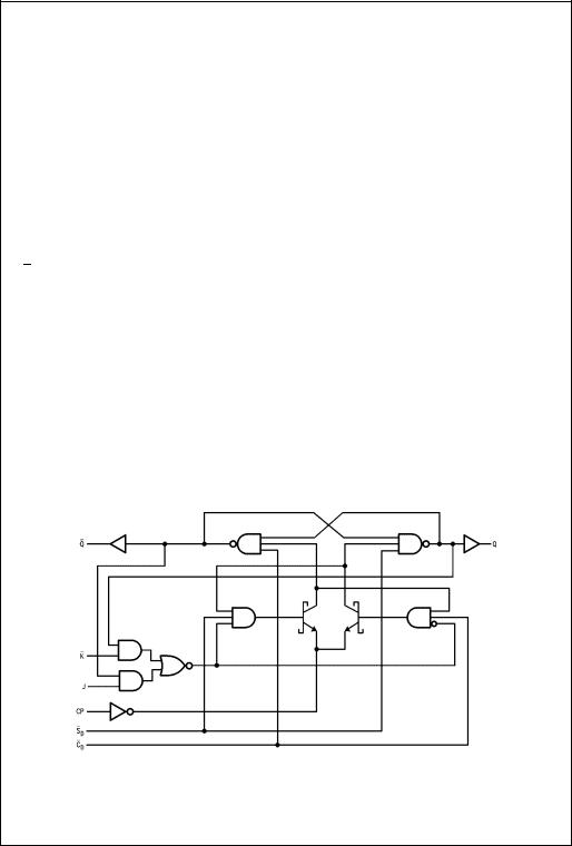
Block Diagram
Please note that this diagram is provided only for the understanding of logic operations and should not be used to estimate propagation delays.
www.fairchildsemi.com |
2 |

Absolute Maximum Ratings(Note 1)
Storage Temperature |
− 65° C to + 150° C |
Ambient Temperature under Bias |
− 55° C to + 125° C |
Junction Temperature under Bias |
− 55° C to + 175° C |
VCC Pin Potential to |
|
Ground Pin |
− 0.5V to + 7.0V |
Input Voltage (Note 2) |
− 0.5V to + 7.0V |
Input Current (Note 2) |
− 30 mA to + 5.0 mA |
Voltage Applied to Output |
|
in HIGH State (with Vcc = 0V) |
|
Standard Output |
− 0.5V to VCC |
3-STATE Output |
− 0.5V to + 5.5V |
Current Applied to Output |
|
in LOW State (Max) |
twice the rated IOL (mA) |
Recommended Operating
Conditions
Free Air Ambient Temperature |
0° C to + 70° C |
Supply Voltage |
+ 4.5V to + 5.5V |
Note 1: Absolute maximum ratings are values beyond which the device may be damaged or have its useful life impaired. Functional operation under these conditions is not implied.
Note 2: Either voltage limit or current limit is sufficient to protect inputs.
DC Electrical Characteristics
Symbol |
Parameter |
|
Min |
Typ |
Max |
Units |
VCC |
|
|
Conditions |
|||||
VIH |
Input HIGH Voltage |
|
2.0 |
|
|
V |
|
Recognized as a HIGH Signal |
|||||||
VIL |
Input LOW Voltage |
|
|
|
0.8 |
V |
|
Recognized as a LOW Signal |
|||||||
VCD |
Input Clamp Diode Voltage |
|
|
|
− 1.2 |
V |
Min |
IIN = |
− 18 mA |
||||||
VOH |
Output HIGH Voltage |
10% VCC |
2.5 |
|
|
V |
Min |
IOH = |
− |
1 mA |
|||||
|
|
5% VCC |
2.7 |
|
|
IOH = |
− |
1 mA |
|||||||
|
|
|
|
|
|
||||||||||
VOL |
Output LOW Voltage |
10% VCC |
|
|
0.5 |
V |
Min |
IOL = |
20 mA |
||||||
IIH |
Input HIGH Current |
|
|
|
5.0 |
µ A |
Max |
VIN = |
2.7V |
||||||
IBVI |
Input HIGH Current Breakdown Test |
|
|
7.0 |
µ A |
Max |
VIN = |
7.0V |
|||||||
ICEX |
Output HIGH Leakage Current |
|
|
50 |
µ A |
Max |
VOUT = |
VCC |
|||||||
VID |
Input Leakage Test |
|
4.75 |
|
|
V |
0.0 |
IID = |
1.9 µ A |
||||||
|
|
|
|
|
All Other Pins Grounded |
||||||||||
|
|
|
|
|
|
|
|
||||||||
|
|
|
|
|
|
|
|
|
|
||||||
IOD |
Output Leakage |
|
|
|
3.75 |
µ A |
0.0 |
VIOD = |
150 mV |
||||||
|
Circuit Current |
|
|
|
All Other Pins Grounded |
||||||||||
|
|
|
|
|
|
|
|||||||||
|
|
|
|
|
|
|
|
|
|
|
|
|
|
||
|
|
|
|
|
− 0.6 |
|
|
VIN = |
|
|
|
|
|
|
|
IIL |
Input LOW Current |
|
|
|
mA |
Max |
0.5V (Jn, Kn) |
||||||||
|
|
|
|
|
− 1.8 |
|
|
VIN = |
|
|
|
|
|
||
|
|
|
|
|
mA |
Max |
0.5V (CDn, SDn) |
||||||||
IOS |
Output Short-Circuit Current |
|
− 60 |
|
− 150 |
mA |
Max |
VOUT = |
0V |
||||||
ICC |
Power Supply Current |
|
|
11.7 |
17.0 |
mA |
Max |
CP = |
0V |
||||||
74F109
3 |
www.fairchildsemi.com |
 Loading...