


74ACTQ652SPC
© 1999 Fairchild Semiconductor Corporation DS010933 www.fairchildsemi.com
June 1991
Revised November 1999
74ACTQ652 Quiet Series Transceiver/Register
74ACTQ652
Quiet Series Transceiver/Register
General Description
The ACTQ652 consists of bus transceiver circuits with D-
type flip-flops, and control circuitry arranged for multiplexed
transmission of data directly from the input bus or from
internal registers. Data on the A or B bus will be clocked
into the registers a s the appropr iate clock pin g oes to the
HIGH logic level. Output Enable pins (OEAB, OEBA
) are
provided to control the transceiver function.
The ACTQ652 utilizes Fairchild FACT Quiet Series tech-
nology to guarantee quiet output switching and improved
dynamic threshold performance. FACT Quiet Series fea-
tures GTO output control and undershoot corrector in
addition to split ground bus for superior performance.
Features
■ Guaranteed simultaneous switching noise level and
dynamic threshold performan ce
■ Guarante ed pin-to-pin skew AC performance
■ Independent registers for A and B buses
■ Multiplexed real-time and stored data
■ Outputs source/sink 24 mA
■ TTL-compatible inputs
Ordering Code:
Device also available in Tape and Reel. Specify by appending s uffix let te r “X” to the ordering code.
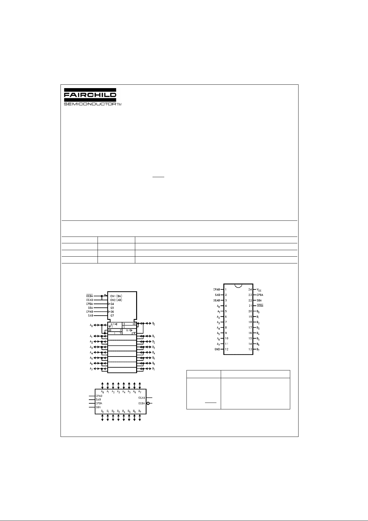
Logic Symbols
IEEE/IEC
Connection Diagram
Pin Descriptions
FACT, Qui et Series , FACT Quiet Series and GTO are trademarks of Fairchild Semiconductor Corporation.
Order Number Package Number Package Description
74ACTQ652SC M24B 24-Lead Small Outline Integrated Circuit (SOIC), JEDEC MS-013, 0.300” Wide Body
74ACTQ652MTC MTC24 24-Lead Thin Shrink Small Outline Package (TSSOP), JEDEC MO-153, 4.4mm Wide
74ACTQ652SPC N24C 24-Lead Plastic Dual-In-Line Package (PDIP), JEDEC MS-100, 0.300” Wide
Pin Names Description
A
0
–A
7
, B
0
–B
7
A and B Inputs/3-STATE Outputs
CPAB, CPBA Clock Inputs
SAB, SBA Select Inputs
OEAB, OEBA
Output Enable Inputs
www.fairchildsemi.com 2
74ACTQ652
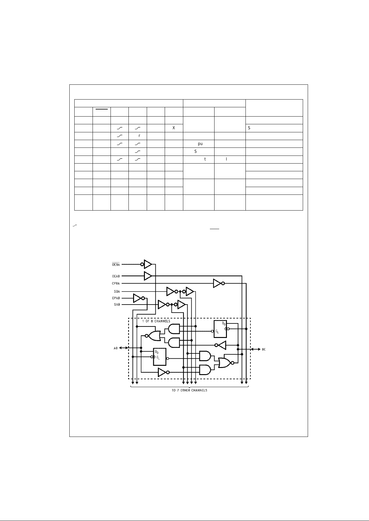
Function Table
H = HIGH Voltage Level
L = LOW Voltage Level
X = Immaterial
= LOW-to-HIGH Clo c k Transi ti on
Note 1: The data output functions may be enabled or dis abled by various signals at OEAB or OEBA
inputs. Data input functions are always enabled,
i.e., data at the bus pins will be stored on every LOW-to-HIGH transition on the clock inputs.
Logic Diagram
Please note that this diagram is provided only for the understanding of logic operations and should not be used to estimate propagation delays.
Inputs Inputs/Outputs (Note 1)
Operating Mode
OEAB OEBA
CPAB CPBA SAB SBA
A
0
thru A
7
B
0
thru B
7
L H H or L H or L X X
Input Input
Isolation
LH
X X Store A and B Data
XH
H or L X X Input Not Specified Store A, Hold B
HH
X X Input Output Store A in Both Registers
LXH or L
X X Not Specified Input Hold A, Store B
LL
X X Output Input Store B in Both Registers
LLXXXL
Output Input
Real-Time B Data to A Bus
L L X H or L X H Store B Data to A Bus
HHXXLX
Input Output
Real-Time A Data to B Bus
H H H or L X H X Stored A Data to B Bus
H L H or L H or L H H Output Output
Stored A Data to B Bus and
Stored B Data to A Bus
3 www.fairchildsemi.com
74ACTQ652
Functional Description
In the transceiver mode , data present a t the HIGH impe d-
ance port may be sto red in either the A or B register or
both.
The select (SAB, SBA) controls can multiplex stored and
real-time.
The examples in Figure 1 de monstr ate the fo ur funda men-
tal bus-management func tions that can be perfor med with
the Octal bus transceivers and receivers.
Data on the A or B data bus, or both can be stored in the
internal D-type flip-flop by LOW-to-H IGH transitions at the
appropriate Clock Inp uts (CPAB, CPBA) regardless of the
Select or Output Enable Inputs. When SAB and SBA are in
the real time transfer m od e, it is a lso po ssibl e to sto re d ata
without using the internal D-type flip-flops by simulta-
neously enabling OEAB and OEBA
. In this configuration
each Output reinforces its Input. Thu s when all other data
sources to the two sets of bus lin es are in a HIGH imp ed-
ance state, each set of bus lines will remain at its last state.
Note A: Real-Time
Transfer Bus B to Bus A
Note C: Storage
Note B: Real-Time
Transfer Bus A to Bus B
Note D: Transfer Storage
Data to A or B
FIGURE 1.
OEAB OEBA
CPAB CPBA SAB SBA
LLXXXL
OEAB OEBA
CPAB CPBA SAB SBA
XH
XXX
LXX
XX
LH
XX
OEAB OEBA CPAB CPBA SAB SBA
HHXXLX
OEAB OEBA
CPAB CPBA SAB SBA
H L H or L H or L H H
 Loading...