


74F113SJX
© 1999 Fairchild Semiconductor Corporation DS009473 www.fairchildsemi.com
April 1988
Revised July 1999
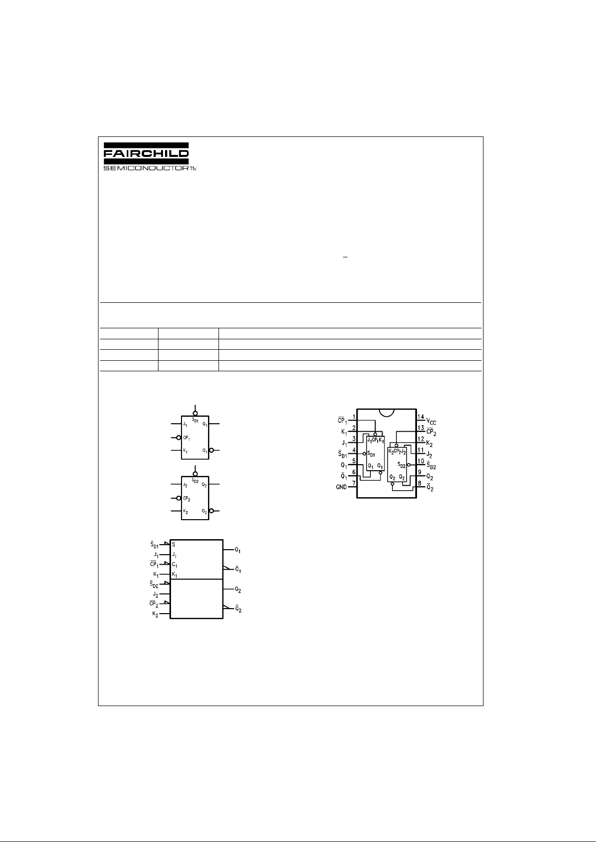
74F113 Dual JK Negative Edge-Triggered Flip-Flop
74F113
Dual JK Negative Edge-Triggered Flip-Flop
General Description
The 74F113 offers individual J, K, Set and Cl ock inputs.
When the clock goes HIGH the inputs are enabled and
data may be entered. The logic level of the J and K inputs
may be changed when the clock pulse is HIGH and the flipflop will perf orm according to the Truth Table as long as
minimum setup and h old tim es are obs erved . Inp ut dat a is
transferred t o the outputs on the falling edge of the clock
pulse.
Asynchronous input:
LOW input to S
D
sets Q to HIGH level
Set is independent of clock
Ordering Code:
Devices also available in Tape and Reel. Specify by appending the suffix letter “X” to the ordering code.
Logic Symbols
IEEE/IEC
Connection Diagram
Order Number Package Number Package Description
74F113SC M14A 14-Lead Small Outline Integrated Circuit (SOIC), JEDEC MS-120, 0.150 Narrow
74F113SJ M14D 14-Lead Small Outline Package (SOP), EIAJ TYPE II, 5.3mm Wide
74F113PC N14A 14-Lead Plastic Dual-In-Line Package (PDIP), JEDEC MS-001, 0.300 Wide
www.fairchildsemi.com 2
74F113
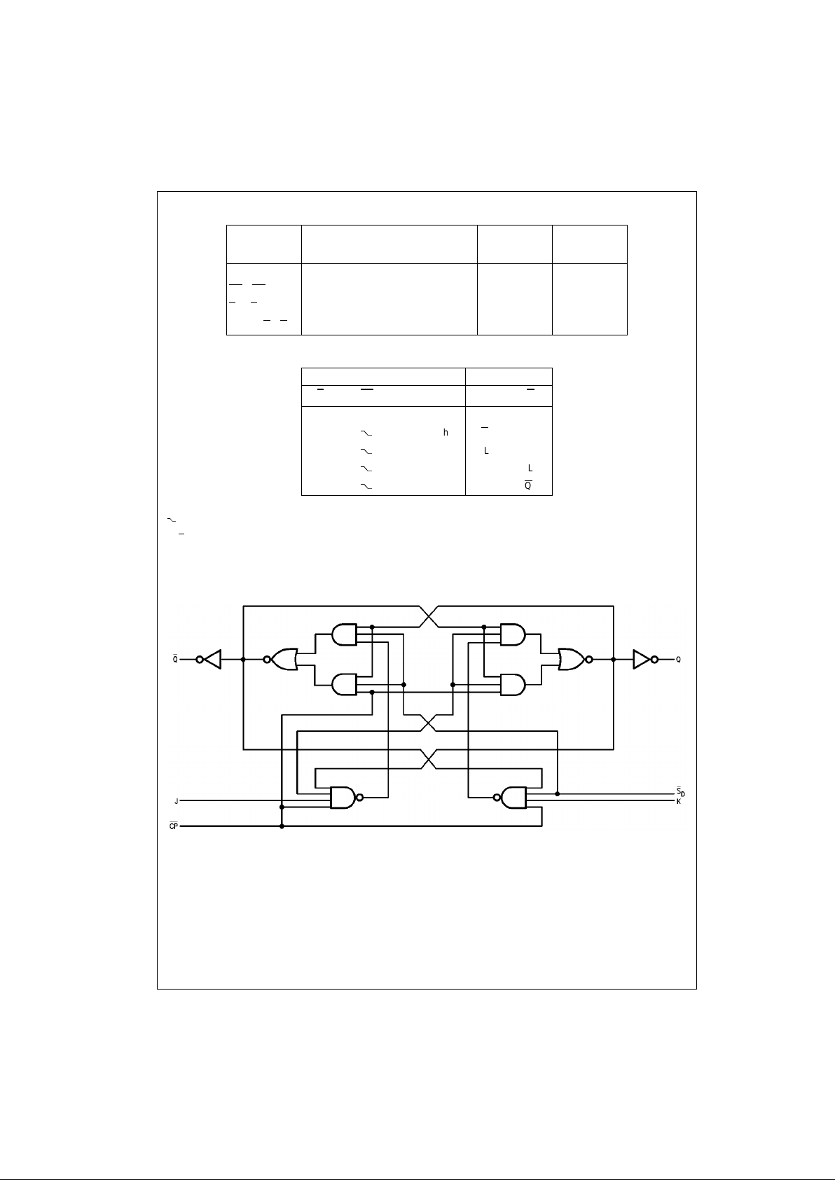
Unit Loading/Fan Out
Tr uth Table
H (h) = HIGH Voltage Level
L (l) = LOW Voltage l evel
]
= HIGH-to-LOW Clock Transition
X = Immaterial
Q
0 (Q0
) = Before HIGH-to-LOW Transition of Clock
Lower case letters indicate the state of the referenced i nput or output prior to the HIGH-to-LOW clock transition.
Logic Diagram
(One Half Shown)
Please note that this diagram is provided only for the understanding of logic operations and should not be use d to estimate propagation delays.
Pin Names Description
U.L.
Input I
IH/IIL
HIGH/LOW
Output I
OH/IOL
J1, J2, K1, K2Data Inputs 1.0/1.0 20 µA/−0.6 mA
CP
1
, CP
2
Clock Pulse Inputs (Active Falling Edge) 1.0/4.0 20 µA/−2.4 mA
S
D1
, S
D2
Direct Set Inputs (Active LOW) 1.0/5.0 20 µA/−3.0 mA
Q
1
, Q2, Q1, Q2Outputs 50/33.3 −1 mA/20 mA
Inputs Outputs
S
D
CP JK Q Q
LXXXHL
H
hhQ0Q
0
H
lhL H
H
hl H L
H
llQ0Q
0
 Loading...