


Fairchild Semiconductor 74ACTQ244CW, 74ACTQ244SJX, 74ACTQ244SJ, 74ACTQ244SCX, 74ACTQ244SC Datasheet
...
July 1989
Revised November 1999
74ACQ244 • 74ACTQ244
Quiet Series Octal Buffer/Line Driver with 3-STATE Outputs
General Description
The ACQ/ACTQ244 is an octal buffer and line driver designed to be employed as a memory address driver, clock driver and bus oriented transmitter or receiver which provides improved PC board density. The ACQ/ACTQ utilizes Fairchild Quiet Series technology to guarantee quiet output switching and improved dynamic threshold performance. FACT Quiet Series features GTO output control and undershoot corrector in addition to a split ground bus for superior performance.
Features
■ICC and IOZ reduced by 50%
■Guaranteed simultaneous switching noise level and dynamic threshold performance
■Guaranteed pin-to-pin skew AC performance
■Improved latch-up immunity
■3-STATE outputs drive bus lines or buffer memory address registers
■Outputs source/sink 24 mA
■Faster prop delays than the standard AC/ACT244
Ordering Code:
Order Number |
Package Number |
Package Description |
|
|
|
74ACQ244SC |
M20B |
20-Lead Small Outline Integrated Circuit (SOIC), JEDEC MS-013, 0.300” Wide Body |
|
|
|
74ACQ244SJ |
M20D |
20-Lead Small Outline Package (SOP), EIAJ TYPE II, 5.3mm Wide |
|
|
|
74ACQ244PC |
N20A |
20-Lead Plastic Dual-In-Line Package (PDIP), JEDEC MS-001, 0.300” Wide |
|
|
|
74ACTQ244SC |
M20B |
20-Lead Small Outline Integrated Circuit (SOIC), JEDEC MS-013, 0.300” Wide Body |
|
|
|
74ACTQ244SJ |
M20D |
20-Lead Small Outline Package (SOP), EIAJ TYPE II, 5.3mm Wide |
|
|
|
74ACTQ244QSC |
MQA20 |
20-Lead Quarter Size Outline Package (QSOP), JEDEC MO-137, 0.150” Wide |
|
|
|
74ACTQ244MSA |
MSA20 |
20-Lead Shrink Small Outline Package (SSOP), EIAJ TYPE II, 5.3mm Wide |
|
|
|
74ACTQ244PC |
N20A |
20-Lead Plastic Dual-In-Line Package (PDIP), JEDEC MS-001, 0.300” Wide |
|
|
|
Device also available in Tape and Reel. Specify by appending suffix letter “X” to the ordering code.
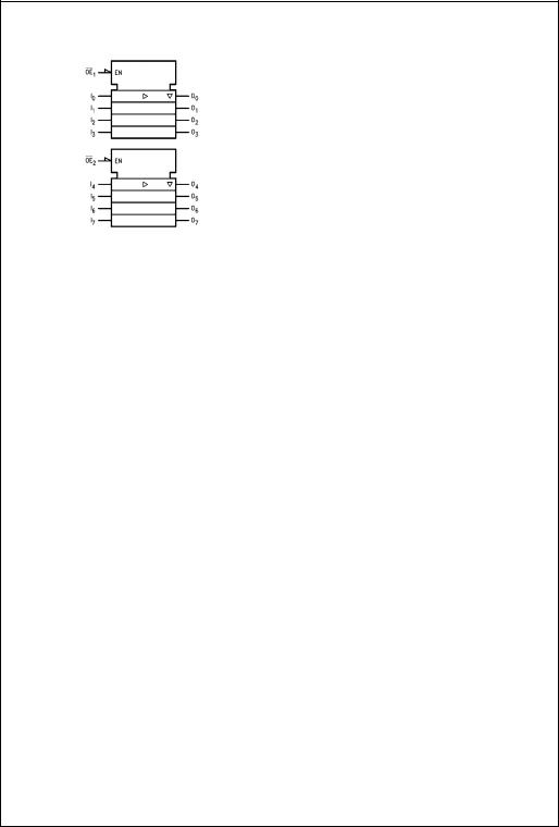
Connection Diagram |
Pin Descriptions |
||||||
|
|
|
|
|
|||
|
|
|
Pin Names |
Description |
|||
|
|
|
|
|
|
|
|
|
|
|
|
1, |
|
2 |
3-STATE Output Enable Inputs |
|
|
|
OE |
OE |
|||
|
|
|
I0–I 7 |
Inputs |
|||
|
|
|
O0–O 7 |
Outputs |
|||
FACT |
, Quiet Series |
, FACT Quiet Series |
, and GTO are trademarks of Fairchild Semiconductor Corporation. |
Outputs STATE-3 with Driver Buffer/Line Octal Series Quiet 74ACTQ244 • 74ACQ244
© 1999 Fairchild Semiconductor Corporation |
DS010235 |
www.fairchildsemi.com |
74ACQ244 • 74ACTQ244
Logic Symbol
IEE/IEC
Truth Tables
|
|
|
|
Inputs |
|
Outputs |
|
|
|
|
|
|
|
|
|
|
|
|
OE1 |
|
In |
(Pins 12, 14, 16, 18) |
|
|
|
|
L |
|
L |
L |
|
|
|
|
|
|
|
|
|
|
|
|
L |
|
H |
H |
|
|
|
|
|
|
|
|
|
|
|
|
H |
|
X |
Z |
|
|
|
|
|
|
|
|
|
|
|
|
|
|
|
|
|
|
|
|
|
Inputs |
|
Outputs |
|
|
|
|
|
|
|
|
|
|
|
|
OE2 |
|
In |
(Pins 3, 5, 7, 9) |
|
|
|
|
L |
|
L |
L |
|
|
|
|
|
|
|
|
|
|
|
|
L |
|
H |
H |
|
|
|
|
|
|
|
|
|
|
|
|
H |
|
X |
Z |
|
|
|
|
|
|
|||
H = HIGH Voltage Level |
|
|
|||||
L = |
LOW Voltage Level |
|
|
||||
X = |
Inmaterial |
|
|
||||
Z = |
HIGH Impedance |
|
|
||||
www.fairchildsemi.com |
2 |

Absolute Maximum Ratings(Note 1)
Supply Voltage (VCC) |
− 0.5V to + 7.0V |
|
DC Input Diode Current (IIK) |
|
|
VI = |
− 0.5V |
− 20 mA |
VI = |
VCC + 0.5V |
+ 20 mA |
DC Input Voltage (VI) |
− 0.5V to VCC + 0.5V |
|
DC Output Diode Current (IOK) |
|
|
VO = |
− 0.5V |
− 20 mA |
VO = |
VCC + 0.5V |
+ 20 mA |
DC Output Voltage (VO) |
− 0.5V to V CC + 0.5V |
|
DC Output Source |
|
|
or Sink Current (IO) |
± 50 mA |
|
DC VCC or Ground Current |
|
|
per Output Pin (I CC or IGND) |
± 50 mA |
|
Storage Temperature (TSTG) |
− 65° C to + 150° C |
|
DC Latch-Up Source or |
|
|
Sink Current |
± 300 mA |
|
Junction Temperature (T J) |
|
|
PDIP |
140° C |
|
Recommended Operating
Conditions
Supply Voltage (VCC) |
|
ACQ |
2.0V to 6.0V |
ACTQ |
4.5V to 5.5V |
Input Voltage (VI) |
0V to VCC |
Output Voltage (VO) |
0V to VCC |
Operating Temperature (TA) |
− 40° C to + 85° C |
Minimum Input Edge Rate ∆ V/∆ t |
|
ACQ Devices |
|
VIN from 30% to 70% of VCC |
|
VCC @ 3.0V, 4.5V, 5.5V |
125 mV/ns |
Minimum Input Edge Rate ∆ V/∆ t |
|
ACTQ Devices |
|
VIN from 0.8V to 2.0V |
|
VCC @ 4.5V, 5.5V |
125 mV/ns |
Note 1: Absolute maximum ratings are those values beyond which damage to the device may occur. The databook specifications should be met, without exception, to ensure that the system design is reliable over its power supply, temperature, and output/input loading variables. Fairchild does not recommend operation of FACT circuits outside databook specifications.
DC Electrical Characteristics for ACQ
Symbol |
Parameter |
VCC |
TA = + 25° C |
|
TA = − 40° C to + 85° C |
Units |
|
|
Conditions |
|||
|
|
|
(V) |
Typ |
|
Guaranteed Limits |
|
|
|
|
|
|
|
|
|
|
|
|
|
|
|
|
|||
VIH |
Minimum HIGH Level |
3.0 |
1.5 |
2.1 |
|
2.1 |
|
VOUT = |
0.1V |
|||
|
Input Voltage |
4.5 |
2.25 |
3.15 |
|
3.15 |
V |
or VCC − |
0.1V |
|||
|
|
|
5.5 |
2.75 |
3.85 |
|
3.85 |
|
|
|
|
|
|
|
|
|
|
|
|
|
|
|
|
||
VIL |
Maximum LOW Level |
3.0 |
1.5 |
0.9 |
|
0.9 |
|
VOUT = |
0.1V |
|||
|
Input Voltage |
4.5 |
2.25 |
1.35 |
|
1.35 |
V |
or VCC − |
0.1V |
|||
|
|
|
5.5 |
2.75 |
1.65 |
|
1.65 |
|
|
|
|
|
|
|
|
|
|
|
|
|
|
|
|
|
|
VOH |
Minimum HIGH Level |
3.0 |
2.99 |
2.9 |
|
2.9 |
|
|
|
|
|
|
|
Output Voltage |
4.5 |
4.49 |
4.4 |
|
4.4 |
V |
IOUT = |
− |
50 µ A |
||
|
|
|
5.5 |
5.49 |
5.4 |
|
5.4 |
|
|
|
|
|
|
|
|
|
|
|
|
|
|
|
|
||
|
|
|
|
|
|
|
|
|
VIN = |
VIL or VIH |
||
|
|
|
3.0 |
|
2.56 |
|
2.46 |
|
IOH = − 12 mA |
|||
|
|
|
4.5 |
|
3.86 |
|
3.76 |
V |
IOH = − 24 mA |
|||
|
|
|
5.5 |
|
4.86 |
|
4.76 |
|
IOH = − 24 mA (Note 2) |
|||
VOL |
Maximum LOW Level |
3.0 |
0.002 |
0.1 |
|
0.1 |
|
|
|
|
|
|
|
Output Voltage |
4.5 |
0.001 |
0.1 |
|
0.1 |
V |
IOUT = |
50 µ A |
|||
|
|
|
5.5 |
0.001 |
0.1 |
|
0.1 |
|
|
|
|
|
|
|
|
|
|
|
|
|
|
|
|
||
|
|
|
|
|
|
|
|
|
VIN = |
VIL or VIH |
||
|
|
|
3.0 |
|
0.36 |
|
0.44 |
|
IOL = 12 mA |
|||
|
|
|
4.5 |
|
0.36 |
|
0.44 |
V |
IOL = 24 mA |
|||
|
|
|
5.5 |
|
0.36 |
|
0.44 |
|
IOL = 24 mA (Note 2) |
|||
IIN |
Maximum Input |
5.5 |
|
± 0.1 |
|
± 1.0 |
µ A |
VI = |
VCC, GND |
|||
(Note 4) |
Leakage Current |
|
|
|||||||||
|
|
|
|
|
|
|
|
|
|
|||
|
|
|
|
|
|
|
|
|
|
|||
IOLD |
Minimum Dynamic |
|
5.5 |
|
|
|
75 |
mA |
VOLD = |
1.65V Max |
||
IOHD |
Output Current (Note 3) |
5.5 |
|
|
|
− 75 |
mA |
VOHD = |
|
3.85V Min |
||
ICC |
Maximum Quiescent |
5.5 |
|
4.0 |
|
40.0 |
µ A |
VIN = |
VCC or GND |
|||
(Note 4) |
Supply Current |
|
|
|||||||||
|
|
|
|
|
|
|
|
|
|
|||
|
|
|
|
|
|
|
|
|
|
|||
IOZ |
Maximum 3-STATE |
|
|
|
|
|
|
VI(OE) = |
VIL, VIH |
|||
|
Leakage Current |
5.5 |
|
± 0.25 |
|
± 2.5 |
µ A |
VI = |
VCC, GND |
|||
|
|
|
|
|
|
|
|
|
VO = |
VCC, GND |
||
74ACTQ244 • 74ACQ244
3 |
www.fairchildsemi.com |
 Loading...