


 Loading...
Analog Devices AD713TQ, AD713SQ, AD713KN, AD713JR-16-REEL7, AD713JR-16-REEL Datasheet
...a |
Quad Precision, Low Cost, |
|
High Speed, BiFET Op Amp |
||
|
|
|
|
|
AD713 |
|
|
|
|
FEATURES |
CONNECTION DIAGRAMS |
|
Enhanced Replacement for LF347 and TL084 |
|
AC PERFORMANCE
1 ms Settling to 0.01% for 10 V Step
20 V/ms Slew Rate
0.0003% Total Harmonic Distortion (THD)
4 MHz Unity Gain Bandwidth
DC PERFORMANCE
0.5 mV max Offset Voltage (AD713K)
20 mV/° C max Drift (AD713K)
200 V/mV min Open Loop Gain (AD713K) 2 mV p-p typ Noise, 0.1 Hz to 10 Hz True 14-Bit Accuracy
Single Version: AD711, Dual Version: AD712 Available in 16-Pin SOIC, 14-Pin Plastic DIP and Hermetic Cerdip Packages
Standard Military Drawing Available
Plastic (N) and |
|
Cerdip (Q) Packages |
SOIC (R) Package |
|
|
|
|
|
|
OUTPUT |
|
OUTPUT |
1 |
|
|
14 |
OUTPUT |
–IN |
|
–IN |
2 |
1 |
4 |
13 |
–IN |
|
+IN |
+IN |
3 |
|
|
12 |
+IN |
|
+VS |
+VS |
4 |
AD713 |
11 |
–VS |
|
+IN |
|
(TOP VIEW) |
|
||||||
|
|
|
|
|
|
||
+IN |
5 |
|
|
10 |
+IN |
|
–IN |
–IN |
6 |
2 |
3 |
9 |
–IN |
OUTPUT |
|
|
|
|
|
|
|
||
OUTPUT |
7 |
|
|
8 |
OUTPUT |
NC |
|
1 |
|
|
16 |
OUTPUT |
|
2 |
1 |
4 |
15 |
–IN |
|
3 |
|
|
14 |
+IN |
|
4 |
AD713 |
13 |
–VS |
||
(TOP VIEW) |
|||||
|
|
|
|||
5 |
|
|
12 |
+IN |
|
6 |
2 |
3 |
11 |
–IN |
|
7 |
|
|
10 |
OUTPUT |
|
8 |
|
|
9 |
NC |
|
NC = NO CONNECT
APPLICATIONS
Active Filters
Quad Output Buffers for 12and 14-Bit DACs Input Buffers for Precision ADCs
Photo Diode Preamplifier Application
PRODUCT DESCRIPTION
The AD713 is a quad operational amplifier, consisting of four AD711 BiFET op amps. These precision monolithic op amps offer excellent dc characteristics plus rapid settling times, high slew rates, and ample bandwidths. In addition, the AD713 provides the close matching ac and dc characteristics inherent to amplifiers sharing the same monolithic die.
The single-pole response of the AD713 provides fast settling:
l s to 0.01%. This feature, combined with its high dc precision, makes the AD713 suitable for use as a buffer amplifier for 12or 14-bit DACs and ADCs. It is also an excellent choice for use in active filters in 12-, 14and 16-bit data acquisition systems. Furthermore, the AD713’s low total harmonic distortion (THD) level of 0.0003% and very close matching ac characteristics make it an ideal amplifier for many demanding audio applications.
The AD713 is internally compensated for stable operation at unity gain and is available in seven performance grades. The AD713J and AD713K are rated over the commercial temperature range of 0° C to 70° C. The AD713A and AD713B are rated over the industrial temperature of –40° C to +85° C. The AD713S and AD713T are rated over the military temperature range of –55° C to +125° C and are available processed to standard microcircuit drawings.
REV. C
Information furnished by Analog Devices is believed to be accurate and reliable. However, no responsibility is assumed by Analog Devices for its use, nor for any infringements of patents or other rights of third parties that may result from its use. No license is granted by implication or otherwise under any patent or patent rights of Analog Devices.
The AD713 is offered in a 16-pin SOIC, 14-pin plastic DIP and hermetic cerdip package.
PRODUCT HIGHLIGHTS
1.The AD713 is a high speed BiFET op amp that offers excellent performance at competitive prices. It upgrades the performance of circuits using op amps such as the TL074, TL084, LT1058, LF347 and OPA404.
2.Slew rate is 100% tested for a guaranteed minimum of 16 V/ s (J, A and S Grades).
3.The combination of Analog Devices’ advanced processing technology, laser wafer drift trimming and well-matched ion-implanted JFETs provides outstanding dc precision. Input offset voltage, input bias current and input offset current are specified in the warmed-up condition and are 100% tested.
4.Very close matching of ac characteristics between the four amplifiers makes the AD713 ideal for high quality active filter applications.
One Technology Way, P.O. Box 9106, Norwood, MA 02062-9106, U.S.A.
Tel: 781/329-4700 |
www.analog.com |
Fax: 781/326-8703 |
© Analog Devices, Inc., 2002 |
AD713–SPECIFICATIONS (VS = 15 V @ TA = 25 C unless otherwise noted)
|
|
|
AD713J/A/S |
|
|
AD713K/B/T |
|
|
|
|
Parameter |
Conditions |
Min |
Typ |
Max |
Min |
Typ |
Max |
Unit |
|
|
|
|
|
|
|
|
|
|
|
|
|
INPUT OFFSET VOLTAGE1 |
|
|
|
|
|
|
|
|
|
|
Initial Offset |
|
|
0.3 |
1.5 |
|
0.2 |
0.5 |
mV |
|
|
Offset |
TMIN to TMAX |
|
0.5 |
2/2/2 |
|
0.4 |
0.7/0.7/1.0 |
mV |
|
|
vs. Temp |
|
78 |
5 |
|
84 |
5 |
20/20/15 |
µ V/° C |
||
vs. Supply |
|
95 |
|
100 |
|
dB |
|
|||
|
TMIN to TMAX |
76/76/76 |
95 |
|
84 |
100 |
|
dB |
|
|
Long-Term Stability |
|
|
15 |
|
|
15 |
|
µ V/Month |
||
INPUT BIAS CURRENT2 |
VCM = 0 V |
|
40 |
150 |
|
40 |
75 |
pA |
|
|
|
VCM = 0 V @ TMAX |
|
|
3.4/9.6/154 |
|
|
1.7/4.8/77 |
nA |
|
|
|
VCM = ± 10 V |
|
55 |
200 |
|
55 |
120 |
pA |
|
|
INPUT OFFSET CURRENT |
VCM = 0 V |
|
10 |
75 |
|
10 |
35 |
pA |
|
|
|
VCM = 0 V @ TMAX |
|
|
1.7/4.8/77 |
|
|
0.8/2.2/36 |
nA |
|
|
MATCHING CHARACTERISTICS |
|
|
|
|
|
|
|
|
|
|
Input Offset Voltage |
|
|
0.5 |
1.8 |
|
0.4 |
0.8 |
mV |
|
|
|
TMIN to TMAX |
|
0.7 |
2.3/2.3/2.3 |
|
0.6 |
1.0/1.0/1.3 |
mV |
|
|
Input Offset Voltage Drift |
|
|
8 |
|
|
6 |
25 |
µ V/° C |
||
Input Bias Current |
|
|
10 |
100 |
|
10 |
35 |
pA |
|
|
Crosstalk |
f = 1 kHz |
|
|
–130 |
|
|
–130 |
dB |
|
|
|
f = 100 kHz |
|
|
–95 |
|
|
–95 |
dB |
|
|
FREQUENCY RESPONSE |
|
|
|
|
|
|
|
|
|
|
Small Signal Bandwidth |
Unity Gain |
3.0 |
4.0 |
|
3.4 |
4.0 |
|
MHz |
||
Full Power Response |
VO = 20 V p-p |
|
200 |
|
|
200 |
|
kHz |
|
|
Slew Rate |
Unity Gain |
16 |
20 |
|
18 |
20 |
|
V/µ s |
|
|
Settling Time to 0.01% |
f = 1 kHz; RL ≥ 2 kΩ ; |
|
1.0 |
1.2 |
|
1.0 |
1.2 |
µ s |
|
|
Total Harmonic Distortion |
|
0.0003 |
|
|
0.0003 |
|
% |
|
||
|
VO = 3 V rms |
|
|
|
|
|
|
|
|
|
INPUT IMPEDANCE |
|
|
3× 10¹² 5.5 |
|
|
3× 10¹² 5.5 |
|
Ω |
pF |
|
Differential |
|
|
|
|
|
|||||
Common Mode |
|
|
3× 10¹² 5.5 |
|
|
3× 10¹² 5.5 |
|
Ω |
pF |
|
INPUT VOLTAGE RANGE |
|
|
± 20 |
|
|
± 20 |
|
|
|
|
Differential3 |
|
|
|
|
|
V |
|
|
||
Common-Mode Voltage4 |
|
|
+14.5, –11.5 |
|
|
+14.5, –11.5 |
|
V |
|
|
|
TMIN to TMAX |
–11 |
|
+13 |
–11 |
|
+13 |
V |
|
|
Common Mode |
VCM = ± 10 V |
78 |
88 |
|
84 |
94 |
|
dB |
|
|
Rejection Ratio |
TMIN to TMAX |
76/76/76 |
84 |
|
82 |
90 |
|
dB |
|
|
|
VCM = ± 11 V |
72 |
84 |
|
78 |
90 |
|
dB |
|
|
|
TMIN to TMAX |
70/70/70 |
80 |
|
74 |
84 |
|
dB |
|
|
INPUT VOLTAGE NOISE |
0.1 Hz to 10 Hz |
|
2 |
|
|
2 |
|
µ V p-p |
||
|
f = 10 Hz |
|
45 |
|
|
45 |
|
nV/√ |
Hz |
|
|
f = 100 Hz |
|
22 |
|
|
22 |
|
nV/√ |
Hz |
|
|
f = 1 kHz |
|
18 |
|
|
18 |
|
nV/√ |
Hz |
|
|
f = 10 kHz |
|
16 |
|
|
16 |
|
nV/√ |
Hz |
|
INPUT CURRENT NOISE |
f = 1 kHz |
|
0.01 |
|
|
0.01 |
|
pA/√ |
Hz |
|
OPEN-LOOP GAIN |
VO = ± 10 V; RL ≥ 2 kΩ |
150 |
400 |
|
200 |
400 |
|
V/mV |
||
|
TMIN to TMAX |
100/100/100 |
|
|
100 |
|
|
V/mV |
||
OUTPUT CHARACTERISTICS |
RL ≥ 2 kΩ |
|
|
|
|
|
|
|
|
|
Voltage |
+13, –12.5 |
+13.9, –13.3 |
|
+13, –12.5 +13.9, –13.3 |
|
V |
|
|
||
|
TMIN to TMAX |
± 12/± 12/ 12 +13.8, –13.1 |
|
12 |
+13.8, –13.1 |
|
V |
|
|
|
Current |
Short Circuit |
|
25 |
|
|
25 |
|
mA |
|
|
POWER SUPPLY |
|
|
± 15 |
|
|
± 15 |
|
|
|
|
Rated Performance |
|
4.5 |
18 |
4.5 |
18 |
V |
|
|
||
Operating Range |
|
|
|
V |
|
|
||||
Quiescent Current |
|
|
10.0 |
13.5 |
|
10.0 |
12.0 |
mA |
|
|
TRANSISTOR COUNT |
# of Transistors |
|
120 |
|
|
120 |
|
|
|
|
NOTES
1Input Offset Voltage specifications are guaranteed after 5 minutes of operation at TA = 25° C.
2Bias Current specifications are guaranteed maximum at either input after 5 minutes of operation at TA = 25° C. For higher temperatures, the current doubles every 10° C. 3Defined as voltage between inputs, such that neither exceeds ± 10 V from ground.
4Typically exceeding –14.1 V negative common-mode voltage on either input results in an output phase reversal.
Specifications subject to change without notice.
–2– |
REV. C |
AD713
ABSOLUTE MAXIMUM RATINGS1, 2
Supply Voltage . . . . . . . . . . . . . . . . . . . . . . . . . . . . . . . . . ±18 V
Internal Power Dissipation2
Input Voltage3 . . . . . . . . . . . . . . . . . . . . . . . . . . . . . . . . . ±18 V Output Short-Circuit Duration
(For One Amplifier) . . . . . . . . . . . . . . . . . . . . . . . . Indefinite Differential Input Voltage . . . . . . . . . . . . . . . . . . +VS and –VS Storage Temperature Range (Q) . . . . . . . . . . –65°C to +150°C Storage Temperature Range (N, R) . . . . . . . . –65°C to +125°C Operating Temperature Range
AD713J/K . . . . . . . . . . . . . . . . . . . . . . . . . . . . . 0°C to 70°C AD713A/B . . . . . . . . . . . . . . . . . . . . . . . . . . –40°C to +85°C AD713S/T . . . . . . . . . . . . . . . . . . . . . . . . . –55°C to +125°C Lead Temperature Range (Soldering 60 sec) . . . . . . . . . . 300°C
NOTES
1Stresses above those listed under “Absolute Maximum Ratings” may cause permanent damage to the device. This is a stress rating only and functional operation of the device at these or any other conditions above those indicated in the operational section of this specification is not implied. Exposure to absolute maximum rating conditions for extended periods may affect device reliability.
2Thermal Characteristics:
14-Pin Plastic Package:
14-Pin Cerdip Package:
θJC = 30°C/
Watt; θJA = 100°C/Watt
3For supply voltages less than ± 18 V, the absolute maximum input voltage is equal to the supply voltage.
ORDERING GUIDE
|
Temperature |
Package |
Package |
Model |
Range |
Description |
Option1 |
AD713AQ |
–40°C to +85°C |
14-Pin Ceramic DIP |
Q-14 |
AD713BQ |
–40°C to +85°C |
14-Pin Ceramic DIP |
Q-14 |
AD713JN |
0°C to 70°C |
14-Pin Plastic DIP |
N-14 |
AD713JR-16 |
0°C to 70°C |
16-Pin Plastic SOIC |
R-16 |
AD713JR-16-REEL |
0°C to 70°C |
16-Pin Plastic SOIC |
R-16 |
AD713JR-16-REEL7 |
0°C to 70°C |
16-Pin Plastic SOIC |
R-16 |
AD713KN |
0°C to 70°C |
14-Pin Plastic DIP |
N-14 |
AD713SQ2 |
–55°C to +125°C |
14-Pin Ceramic DIP |
Q-14 |
AD713TQ2 |
–55°C to +125°C |
14-Pin Ceramic DIP |
Q-14 |
5962-9063301MCA |
–55°C to +125°C |
14-Pin Ceramic DIP |
Q-14 |
5962-9063302MCA2 |
–55°C to +125°C |
14-Pin Ceramic DIP |
Q-14 |
1N = Plastic DIP; Q = Cerdip; R = Small Outline IC (SOIC). 2Not for new designs. Obsolete April 2002.
CAUTION
ESD (electrostatic discharge) sensitive device. Electrostatic charges as high as 4000 V readily accumulate on the human body and test equipment and can discharge without detection. Although the AD713 features proprietary ESD protection circuitry, permanent damage may occur on devices subjected to high-energy electrostatic discharges. Therefore, proper ESD precautions are recommended to avoid performance degradation or loss of functionality.
WARNING!
ESD SENSITIVE DEVICE
REV. C |
–3– |
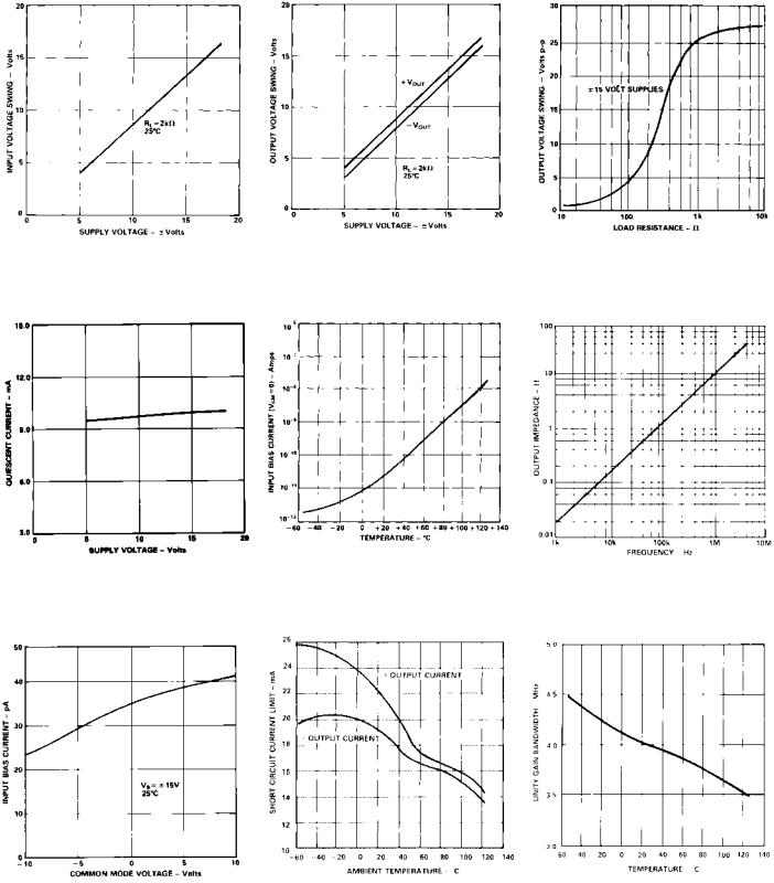
AD713–Typical Performance Characteristics
TPC 1. Input Voltage Swing vs. Supply Voltage
TPC 4. Quiescent Current vs. Supply Voltage
TPC 7. Input Bias Current vs. Common Mode Voltage
TPC 2. Output Voltage Swing vs. Supply Voltage
TPC 5. Input Bias Current vs. Temperature
TPC 8. Short-Circuit Current Limit vs. Temperature
TPC 3. Output Voltage Swing vs. Load Resistance
TPC 6. Output Impedance vs. Frequency, G = 1
TPC 9. Gain Bandwidth Product vs. Temperature
–4– |
REV. C |

Typical Performance Characteristics–AD713
TPC 10. Open-Loop Gain and Phase Margin vs. Frequency
TPC 13. Common Mode Rejection vs. Frequency
TPC 16. Total Harmonic Distortion vs. Frequency
TPC 11. Open-Loop Gain vs. Supply Voltage
TPC 14. Large Signal Frequency
Response
TPC 17. Input Noise Voltage
Spectral Density
TPC 12. Power Supply Rejection vs. Frequency
TPC 15. Output Swing and Error vs. Settling Time
TPC 18. Slew Rate vs. Input Error Signal
REV. C |
–5– |
Loading...