


SN65LBC031Q HIGH-SPEED CONTROLLER AREA NETWORK (CAN) TRANSCEIVERS
SLRS048B ± MAY 1998 ± REVISED MAY 2000
DSN65LBC031Q Meets Standard ISO/DIS 11898 (up to 500 k Baud)
DDriver Output Capability at 50 mA
DWide Positive and Negative Input/output Bus Voltage Range
DBus Outputs Short-Circuit-Protected to Battery Voltage and Ground
D PACKAGE (TOP VIEW)
|
|
|
|
|
|
|
|
|
|
TX |
|
1 |
8 |
|
ASC |
||
GND |
|
|
2 |
7 |
|
CANH |
||
VCC |
|
|
3 |
6 |
|
CANL |
||
RX |
|
|
4 |
5 |
|
REF |
||
|
|
|
|
|
|
|
|
|
D D
Thermal Shutdown
Available in Q-Temp Automotive
±High Reliability Automotive Applications
±Configuration Control/Print Support
±Qualification to Automotive Standards
description |
|
REF |
Reference output |
|
|
|
|
|||
The SN65LBC031Q is a CAN transceiver used as |
|
CANL |
Low side bus output driver |
|
|
|
||||
|
CANH |
High side bus output driver |
|
|
|
|||||
an interface between a CAN controller and the |
|
|
|
|
||||||
|
ASC |
Adjustable slope control |
|
|
|
|||||
physical bus for high speed applications of up to |
|
|
|
|
||||||
|
|
|
|
|
|
|
|
|
|
|
500 k Baud. The device provides transmit |
|
|
|
|
FUNCTION TABLE |
|
|
|
|
|
capability to the differential bus and differential |
|
|
TX |
|
CANH |
CANL |
BUS STATE |
|
RX |
|
receive capability to the controller. The transmitter |
|
|
|
|
|
|
|
|
||
|
|
L |
H |
L |
Dominant |
|
L |
|||
outputs (CANH and CANL), feature internal |
|
|
|
|
|
|
|
|||
High or floating |
Floating |
Floating |
Recessive |
|
H |
|||||
transition regulation to provide controlled |
|
|
|
|
|
|
|
|
|
|
L = low, H = high |
|
|
|
|
|
|||||
symmetry resulting in low EMI emissions. Both |
|
|
|
|
|
|||||
|
|
|
|
|
|
|
|
|
|
|
transmitter outputs are fully protected against battery short circuits and electrical transients that can occur on the bus lines. In the event of excessive device power dissipation the output drivers are disabled by the thermal shutdown circuitry at a junction temperature of approximately 160°C. The inclusion of an internal pullup resistor on the transmitter input ensures a defined output during power up and protocol controller reset. For normal operation at 500 k Baud the ASC terminal is open or tied to GND. For slower speed operation at 125 k Baud the bus output transition times can be increased to reduce EMI by connecting the ASC terminal to VCC. The receiver includes an integrated filter that suppresses the signal into pulses less than 30 ns wide.
The SN65LBC031Q is characterized for operation over the automotive temperature range of ±40°C to 125°C.
logic diagram
VCC |
|
|
ASC |
R |
R |
|
R3 |
CANH |
TX |
|
|
|
CANL |
|
|
|
|
R2 |
R1 |
2R |
REF |
|
2R |
|
R1 |
|
|
|
|
RX |
|
|
|
R |
R |
|
|
GND |
Please be aware that an important notice concerning availability, standard warranty, and use in critical applications of Texas Instruments semiconductor products and disclaimers thereto appears at the end of this data sheet.
PRODUCTION DATA information is current as of publication date. Products conform to specifications per the terms of Texas Instruments standard warranty. Production processing does not necessarily include testing of all parameters.
Copyright 2000, Texas Instruments Incorporated
POST OFFICE BOX 655303 •DALLAS, TEXAS 75265 |
1 |
SN65LBC031Q
HIGH-SPEED CONTROLLER AREA NETWORK (CAN) TRANSCEIVERS
SLRS048B ± MAY 1998 ± REVISED MAY 2000
absolute maximum ratings over operating free-air temperature range (unless otherwise noted)²
Logic supply voltage, VCC (see Note 1) . . . . . . . . . . . . . . . . . . . . . . . . . . . . . . . |
. . . . . . . . . . . . . . . . . . . . . . . . . 7 |
V |
||||
Bus terminal voltage . . . . . . . . . . . . . . . . . . . . . . . . . . . . . . . . . . . . . . . . . . . . . . . . |
. . . . . . . . . . . . . . . . . ±5 V to 20 |
V |
||||
Input current at |
TX |
|
. . . . . . . . . . . . . . . . . . . . . . . . . . . . . . .and ASC terminal, II |
. . . . . . . . . . . . . . . . . . . . . ±10 mA |
||
Input voltage at |
TX |
. . . . . . . . . . . . . . . . . . . . . . . . . . . . . .and ASC terminal, VI |
. . . . . . . . . . . . . . . . . . . . . 2 × VCC |
|||
Operating free-air temperature range, TA . . . . . . . . . . . . . . . . . . . . . . . . . . . . |
. . . . . . . . . . . . . . ±40°C to125°C |
|||||
Operating junction temperature range, TJ . . . . . . . . . . . . . . . . . . . . . . . . . . . . . |
. . . . . . . . . . . . . . ±40°C to 150°C |
|||||
Continuous total power dissipation at (or below) 25°C free-air temperature |
. . See Dissipation Rating Table |
|||||
Storage temperature range, Tstg . . . . . . . . . . . . . . . . . . . . . . . . . . . . . . . . . . . . . |
. . . . . . . . . . . . . . ±65°C to 150°C |
|||||
Case temperature for 10 sec TC, D package . . . . . . . . . . . . . . . . . . . . . . . . . . |
. . . . . . . . . . . . . . . . . . . . . . 260°C |
|||||
² Stresses beyond those listed under ªabsolute maximum ratingsº may cause permanent damage to the device. These are stress ratings only, and functional operation of the device at these or any other conditions beyond those indicated under ªrecommended operating conditionsº is not implied. Exposure to absolute-maximum-rated conditions for extended periods may affect device reliability.
NOTE 1: All voltage values, except differential bus voltage, are measured with respect to GND.
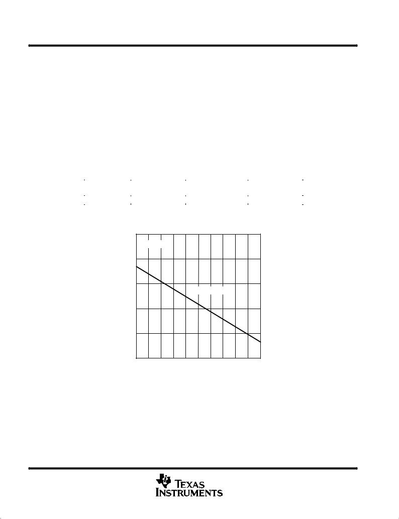
DISSIPATION RATING TABLE
PACKAGE |
TA ≤ 25°C |
OPERATING FACTOR |
TC = 125°C |
|
POWER RATING |
ABOVE TC = 25°C |
POWER RATING |
||
|
||||
D |
725 mW |
5.8 mW/°C |
145 mW |
PD ± Maximum Continuous Dissipation ± mW
DISSIPATION DERATING CURVE vs
FREE-AIR TEMPERATURE
1000
TC = 25°C
800
600
D = 5.8 mW/°C
400
200
0
25 |
35 |
45 |
55 |
65 |
75 |
85 |
95 |
105 |
115 |
125 |
|
|
TA ± Free-Air Temperature ± °C |
|
|
||||||
Figure 1
2 |
POST OFFICE BOX 655303 •DALLAS, TEXAS 75265 |
SN65LBC031Q HIGH-SPEED CONTROLLER AREA NETWORK (CAN) TRANSCEIVERS
SLRS048B ± MAY 1998 ± REVISED MAY 2000
recommended operating conditions
|
|
|
|
|
MIN |
NOM |
MAX |
UNIT |
|
|
|
|
|
|
|
|
|
Logic supply voltage, VCC |
|
|
|
4.5 |
5 |
5.5 |
V |
|
Voltage at any bus terminal (separately or common mode), VI or VIC (see Note 3) |
±2 |
|
7 |
V |
||||
High-level input voltage, VIH |
|
TX |
|
|
2 |
|
VCC |
V |
Low-level input voltage, VIL |
|
|
|
|
0 |
|
0.8 |
V |
|
TX |
|
|
|||||
High-level output current, IOH |
|
Transmitter |
|
|
±50 |
mA |
||
|
|
|
|
|
|
|
|
|
|
Receiver |
|
|
±400 |
µA |
|||
|
|
|
|
|||||
Low-level output current, IOL |
|
Transmitter |
|
|
50 |
mA |
||
|
|
|
|
|
|
|
||
|
Receiver |
|
|
1 |
||||
|
|
|
|
|
||||
|
|
|
|
|
|
|
|
|
Operating free-air temperature, TA |
|
|
|
±40 |
|
125 |
°C |
|
NOTES: 2. All voltage values, except differential bus voltage, are measured with respect to the ground terminal. |
|
|
|
|||||
3. For bus voltages from ±5 V to ±2 V and 7 V to 20 V the receiver output is stable. |
|
|
|
|
||||
SYMBOL DEFINITION
DATA SHEET PARAMETER |
DEFINITION |
|
|
VO(CANHR) |
CANH bus output voltage (recessive state) |
VO(CANLR) |
CANL bus output voltage (recessive state) |
VO(CANHD) |
CANH bus output voltage (dominant state) |
VO(CANLD) |
CANL bus output voltage (dominant state) |
VO(DIFFR) |
Bus differential output voltage (recessive state) |
VO(DIFFD) |
Bus differential output voltage (dominant state) |
VI(ASC) |
Adjustable slope control input voltage |
electrical characteristics over recommended ranges of supply voltage and operating free-air temperature (unless otherwise noted)
|
PARAMETER |
TEST CONDITIONS |
MIN |
TYP |
MAX |
UNIT |
|
|
|
|
|
|
|
VO(REF) |
Reference source output voltage |
IREF = ± 20 µA |
0.45VCC |
|
0.55VCC |
V |
RO(REF) |
Reference source output resistance |
|
5 |
|
10 |
kΩ |
ICC(REC) |
Logic supply current, recessive state |
See Figure 2, S1 closed |
|
12 |
20 |
mA |
ICC(DOM) |
Logic supply current, dominant state |
|
55 |
80 |
||
|
|
|
POST OFFICE BOX 655303 •DALLAS, TEXAS 75265 |
3 |
 Loading...