


SN65240P
Texas Instruments SN65240P, SN65240PW, SN65240PWR, SN65220DBVR, SN65220DBVT Datasheet
...
SN65220, SN65240, SN75240
SINGLE AND DUAL UNIVERSAL SERIAL BUS PORT
TRANSIENT SUPPRESSORS
SLLS266C – FEBRUARY 1997 – REVISED MARCH 2000
1
POST OFFICE BOX 655303 • DALLAS, TEXAS 75265
D
Design to Protect Submicron 3-V or 5-V
Silicon from Noise Transients
D
Applicable to Two High- or Low-Speed
Universal Serial Bus (USB) Host, Hub, or
Peripheral Ports
D
Port ESD Protection Capability Exceeds:
– 15-kV Human Body Model
– 2-kV Machine Model
D
Low Current Leakage ...1 µA Max
D
Stand-Off Voltage . . . 6.0 V Min
D
Low Capacitance . . . 35 pF Typ
description
The SN65220 is a single transient voltage
suppressor and the SN75240 and SN65240 are
dual transient voltage suppressors designed to
provide additional electrical noise transient
protection to two USB ports. Any cabled I/O can
be subjected to electrical noise transients from
various sources. These noise transients can
cause damage to the USB transceiver and/or the
USB ASIC if they are of sufficient magnitude and
duration. The USB ports are typically implement-
ed in 3-V or 5-V digital CMOS with very limited
ESD protection. The SN65220, SN75240, and
SN65240 can significantly increase the port ESD
protection level and reduce the risk of damage to
the large and expensive circuits of the USB port.
The SN75240 is characterized for operation from
0°C to 70°C. The SN65220 and SN65240 are
characterized for operation from –40°C to 85°C.
IEC1000-4-2 ESD performance is measured at
the system level and system design influences the
results of these tests. A high compliance level may
be attained with proper system design.
IEC1000-4-2 Compliance T est Levels
MAXIMUM TEST VOLTAGE
IEC1000
-
4
-
2
COMPLIANCE
LEVEL
CONTACT
DISCHARGE
(kV)
AIR
DISCHARGE
(kV)
1 2 2
2 4 4
3 6 8
4 8 15
Copyright 2000, Texas Instruments Incorporated
PRODUCTION DATA information is current as of publication date.
Products conform to specifications per the terms of Texas Instruments
standard warranty. Production processing does not necessarily include
testing of all parameters.
Please be aware that an important notice concerning availability, standard warranty, and use in critical applications of
Texas Instruments semiconductor products and disclaimers thereto appears at the end of this data sheet.
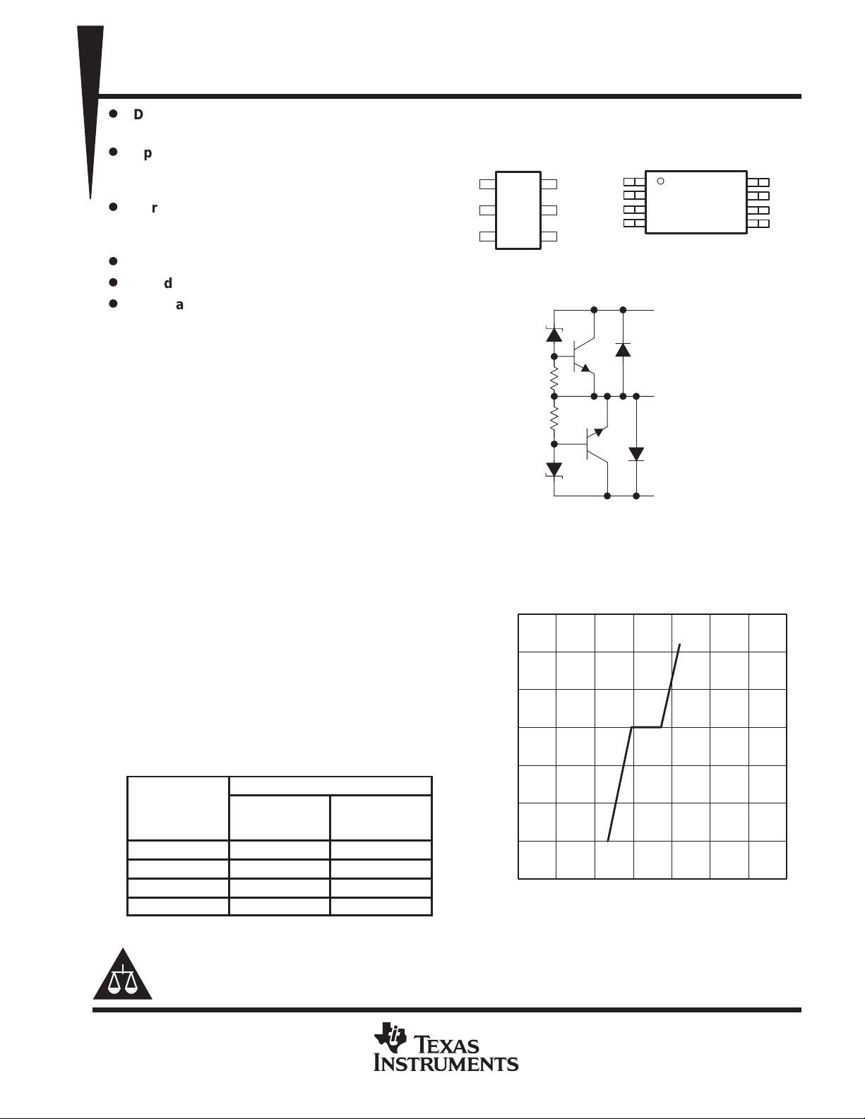
schematic
A or C
GND
B or D
(One Suppressor Shown)
NOTE A: All four GND terminals should be connected to ground.
3
2
4
6
(TOP VIEW)
1
NC
GND
NC
A
B
SN65220
(Marked as SADI)
DBV PACKAGE
GND
5
NC – No internal connection
1
2
3
4
8
7
6
5
GND
C
GND
D
A
GND
B
GND
SN65240, SN75240
(Marked as A65240 or A75240)
P OR PW PACKAGE
(TOP VIEW)
NOTE A: Typical current versus voltage curve was derived
using the IEC 1.2/50-µs surge waveform.
CURRENT
vs
VOLTAGE
–2.5
–5
–7.5
–10
–10 0
0
2.5
5
10
20 30
Voltage – V
Current – A
–20–30 40
7.5
SN65220, SN65240, SN75240
SINGLE AND DUAL UNIVERSAL SERIAL BUS PORT
TRANSIENT SUPPRESSORS
SLLS266C – FEBRUARY 1997 – REVISED MARCH 2000
2
POST OFFICE BOX 655303 • DALLAS, TEXAS 75265
absolute maximum ratings over operating free-air temperature range (unless otherwise noted)
†
Continuous total power dissipation See Dissipation Rating Table. . . . . . . . . . . . . . . . . . . . . . . . . . . . . . . . . . . . .
Electrostatic discharge Class 3, A:15 kV, B: 2 kV. . . . . . . . . . . . . . . . . . . . . . . . . . . . . . . . . . . . . . . . . . . . . . . . . . . .
Peak power dissipation, P
D(peak)
60 W. . . . . . . . . . . . . . . . . . . . . . . . . . . . . . . . . . . . . . . . . . . . . . . . . . . . . . . . . . .
Peak forward surge current, I
FSM
3 A. . . . . . . . . . . . . . . . . . . . . . . . . . . . . . . . . . . . . . . . . . . . . . . . . . . . . . . . . . . . .
Peak reverse surge current, I
RSM
–9 A. . . . . . . . . . . . . . . . . . . . . . . . . . . . . . . . . . . . . . . . . . . . . . . . . . . . . . . . . . . .
Storage temperature range, T
stg
–65°C to 150°C. . . . . . . . . . . . . . . . . . . . . . . . . . . . . . . . . . . . . . . . . . . . . . . . . . .
Lead temperature 1,6 mm (1/16 inch) from case for 10 seconds 260°C. . . . . . . . . . . . . . . . . . . . . . . . . . . . . . .
†
Stresses beyond those listed under “absolute maximum ratings” may cause permanent damage to the device. These are stress ratings only, and
functional operation of the device at these or any other conditions beyond those indicated under “recommended operating conditions” is not
implied. Exposure to absolute-maximum-rated conditions for extended periods may affect device reliability.
DISSIPATION RATING TABLE
PACKAGE
T
A
≤ 25°C
POWER RATING
DERATING FACTOR
ABOVE T
A
= 25°C
T
A
= 70°C
POWER RATING
T
A
= 85°C
POWER RATING
DBV 385 mW 3.1 mW/°C 246 mW 200 mW
P 1150 mW 9.2 mW/°C 736 mW 598 mW
PW 520 mW 4.2 mW/°C 331 mW 268 mW
‡
This is the inverse of the junction-to-ambient thermal resistance when board-mounted and with no air flow.
recommended operating conditions
MIN MAX UNIT
p
p
SN65240, SN65220 –40 85
°
Operating
free
-
air
temperat
u
re
,
T
A
SN75240 0 70
°C
electrical characteristics over recommended operating conditions (unless otherwise noted)
PARAMETER TEST CONDITIONS MIN TYP MAX UNIT
I
lkg
Leakage current V
I
= 6 V at A, B, C, or D terminals 1 µA
V
(BR)
Breakdown voltage V
I
= 1 mA at A, B, C, or D terminals 7 V
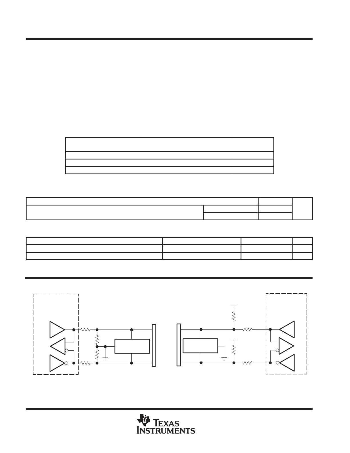
APPLICATION INFORMATION
GND
15 kΩ
15 kΩ
27 Ω
27 Ω
GND
SN65220 or
1/2 SNx5240
A
B
D+
D–
Full-Speed or
Low-Speed USB
Host-or-Hub Port
Transceiver
1.5 kΩ
(Low Speed
Only)
27 Ω
27 Ω
SN65220 or
1/2 SNx5240
A
B
D+
D–
Full-Speed or
Low-Speed USB
Down Stream
Transceiver
1.5 kΩ
(Full Speed Only)
Figure 1. Typical USB Application
 Loading...