


Texas Instruments SN54ALS541J, SN74ALS540N3, SN74ALS541-1DW, SN74ALS541-1N, SN74ALS541DBR Datasheet
...
|
SN54ALS541, SN74ALS540, SN74ALS541 |
||||||
|
OCTAL BUFFERS AND LINE DRIVERS |
||||||
|
|
|
WITH 3-STATE OUTPUTS |
||||
|
|
SDAS025C ± APRIL 1982 ± REVISED JANUARY 1995 |
|||||
• 3-State Outputs Drive Bus Lines or Buffer |
SN54ALS541 . . . J PACKAGE |
||||||
Memory Address Registers |
SN74ALS540, SN74ALS541 . . . DW OR N PACKAGE |
||||||
• pnp Inputs Reduce dc Loading |
|
(TOP VIEW) |
|
|
|||
|
|
|
|
|
|
|
|
• Data Flow-Through Pinout (All Inputs on |
|
OE1 |
1 |
|
20 |
VCC |
|
Opposite Side From Outputs) |
|
|
|
||||
|
A1 |
2 |
|
19 |
OE2 |
|
|
• Package Options Include Plastic |
|
A2 |
3 |
|
18 |
Y1 |
|
Small-Outline (DW) Packages, Ceramic |
|
A3 |
4 |
|
17 |
Y2 |
|
Chip Carriers (FK), and Standard Plastic (N) |
|
A4 |
5 |
|
16 |
Y3 |
|
and Ceramic (J) 300-mil DIPs |
|
A5 |
6 |
|
15 |
Y4 |
|
description |
|
A6 |
7 |
|
14 |
Y5 |
|
|
A7 |
8 |
|
13 |
Y6 |
|
|
These octal buffers and line drivers are designed |
|
A8 |
9 |
|
12 |
Y7 |
|
|
GND |
10 |
|
11 |
Y8 |
|
|
to have the performance of the popular |
|
|
|
||||
|
|
|
|
|
|
|
|
SN54ALS240A/SN74ALS240A series and, at the |
|
|
|
|
|
|
|
same time, offer a pinout with inputs and outputs |
SN54ALS541 . . . FK PACKAGE |
||||||
on opposite sides of the package. This |
|
|
(TOP VIEW) |
|
|||
arrangement greatly facilitates printed-circuit- |
|
A2 |
A1 |
OE1 |
V |
OE2 |
|
board layout. |
|
|
|||||
|
|
|
|
|
CC |
|
|
The 3-state control gate is a 2-input NOR such that |
A3 |
3 |
2 |
1 |
20 19 |
Y1 |
|
if either output-enable (OE1 or OE2) input is high, |
4 |
|
|
|
18 |
||
all eight outputs are in the high-impedance state. |
A4 |
5 |
|
|
|
17 |
Y2 |
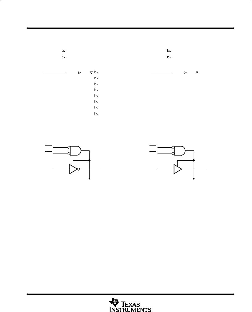
The SN74ALS540 provides inverted data. The |
A5 |
6 |
|
|
|
16 |
Y3 |
A6 |
7 |
|
|
|
15 |
Y4 |
|
′ALS541 provide true data at the outputs. |
|
|
|
||||
A7 |
8 |
|
|
|
14 |
Y5 |
|
|
|
|
|
||||
The -1 versions of SN74ALS540 and |
|
9 |
10 11 12 13 |
|
|||
|
|
|
|
|
|
|
|
SN74ALS541 are identical to the standard |
|
A8 |
GND |
Y8 |
Y7 |
Y6 |
|
versions, except that the recommended maximum |
|
|
|||||
IOL is increased to 48 mA. There is no -1 version |
|
|
|
|
|
|
|
of the SN54ALS541. |
|
|
|
|
|
|
|
The SN54ALS541 is characterized for operation over the full military temperature range of ±55°C to 125°C. The SN74ALS540 and SN74ALS541 are characterized for operation from 0°C to 70°C.
PRODUCTION DATA information is current as of publication date. Products conform to specifications per the terms of Texas Instruments standard warranty. Production processing does not necessarily include testing of all parameters.
Copyright 1995, Texas Instruments Incorporated
POST OFFICE BOX 655303 •DALLAS, TEXAS 75265 |
1 |
SN54ALS541, SN74ALS540, SN74ALS541
OCTAL BUFFERS AND LINE DRIVERS
WITH 3-STATE OUTPUTS
SDAS025C ± APRIL 1982 ± REVISED JANUARY 1995
logic symbols²
|
|
|
|
|
SN74ALS540 |
|
|
|
|
|
|
|
′ALS541 |
||||||
|
1 |
|
|
|
|
|
|
|
|
|
1 |
|
|
|
|
|
|
||
|
|
& |
|
|
|
|
|
|
& |
|
|
|
|
||||||
OE1 |
|
|
|
|
|
EN |
|
|
|
OE1 |
|
|
|
|
EN |
|
|
||
|
|
|
|
|
|
|
|
|
|
|
|||||||||
|
19 |
|
|
|
|
|
|
|
19 |
|
|
|
|||||||
OE2 |
|
|
|
|
|
|
|
|
OE2 |
|
|
|
|
|
|
|
|||
|
|
|
|
|
|
|
|
|
|
|
|
|
|
|
|||||
2 |
|
|
|
|
|
|
18 |
|
2 |
|
|
|
|
18 |
|
||||
|
|
|
|
|
|
|
|
|
|
|
|
||||||||
|
|
|
|
|
|
|
|
|
|
|
|
||||||||
|
|
|
|
|
|
|
|
|
|
|
|||||||||
A1 |
|
|
|
|
|
|
Y1 |
A1 |
|
|
|
|
|
Y1 |
|||||
|
|
|
|
|
|
|
|||||||||||||
3 |
|
|
|
|
|
17 |
|
3 |
|
|
17 |
|
|||||||
|
|
|
|
|
|
|
|
||||||||||||
A2 |
|
|
|
|
|
|
|
Y2 |
A2 |
|
|
|
|
|
|
Y2 |
|||
|
|
|
|
|
|
|
|
|
|||||||||||
4 |
|
|
|
|
|
16 |
|
4 |
|
|
16 |
|
|||||||
|
|
|
|
|
|
|
|
||||||||||||
A3 |
|
|
|
|
|
|
|
Y3 |
A3 |
|
|
|
|
|
|
Y3 |
|||
|
|
|
|
|
|
|
|
|
|||||||||||
5 |
|
|
|
|
|
15 |
|
5 |
|
|
15 |
|
|||||||
|
|
|
|
|
|
|
|
||||||||||||
A4 |
|
|
|
|
|
|
|
Y4 |
A4 |
|
|
|
|
|
|
Y4 |
|||
|
|
|
|
|
|
|
|
|
|||||||||||
6 |
|
|
|
|
|
14 |
|
6 |
|
|
14 |
|
|||||||
|
|
|
|
|
|
|
|
||||||||||||
A5 |
|
|
|
|
|
|
|
Y5 |
A5 |
|
|
|
|
|
|
Y5 |
|||
|
|
|
|
|
|
|
|
|
|||||||||||
7 |
|
|
|
|
|
13 |
|
7 |
|
|
13 |
|
|||||||
|
|
|
|
|
|
|
|
||||||||||||
A6 |
|
|
|
|
|
|
|
Y6 |
A6 |
|
|
|
|
|
|
Y6 |
|||
|
|
|
|
|
12 |
|
12 |
||||||||||||
8 |
|
|
|
|
|
Y7 |
8 |
|
|
Y7 |
|||||||||
|
|
|
|
|
|
|
|||||||||||||
A7 |
|
|
|
|
|
|
|
A7 |
|
|
|
|
|
|
|||||
|
|
|
|
|
|
|
|
|
|||||||||||
9 |
|
|
|
|
|
11 |
|
9 |
|
|
11 |
|
|||||||
|
|
|
|
|
|
|
|
||||||||||||
A8 |
|
|
|
|
|
|
|
Y8 |
A8 |
|
|
|
|
|
|
Y8 |
|||
|
|
|
|
|
|
|
|
|
|||||||||||
² These symbols are in accordance with ANSI/IEEE Std 91-1984 and IEC Publication 617-12.
logic diagrams (positive logic)
|
1 |
SN74ALS540 |
|
1 |
′ALS541 |
OE1 |
|
OE1 |
|
||
|
|
|
|
||
OE2 |
19 |
|
OE2 |
19 |
|
|
|
|
|
||
A1 |
2 |
18 |
A1 |
2 |
18 |
|
Y1 |
|
Y1 |
||
|
|
To Seven Other Channels |
|
|
To Seven Other Channels |
absolute maximum ratings over operating free-air temperature range (unless otherwise noted)³
Supply voltage, VCC . . . . . . . . . . . . . . . . . . . . . . . . . . . . . . . . . . . . . . . . . . . . . . . . . . . . . . . . . . . . . |
. . . . . . . . . . . 7 |
V |
Input voltage, VI . . . . . . . . . . . . . . . . . . . . . . . . . . . . . . . . . . . . . . . . . . . . . . . . . . . . . . . . . . . . . . . . . . |
. . . . . . . . . . 7 |
V |
Voltage applied to a disabled 3-state output . . . . . . . . . . . . . . . . . . . . . . . . . . . . . . . . . . . . . . . . . . |
. . . . . . . . 5.5 |
V |
Operating free-air temperature range, TA: SN54ALS541 . . . . . . . . . . . . . . . . . . . . . . . . . . . . . |
±55°C to 125°C |
|
SN74ALS540, SN74ALS541 . . . . . . . . . . . . . . . . . . |
. . 0°C to 70°C |
|
Storage temperature range . . . . . . . . . . . . . . . . . . . . . . . . . . . . . . . . . . . . . . . . . . . . . . . . . . . . . . . |
±65°C to 150°C |
|
³Stresses beyond those listed under ªabsolute maximum ratingsº may cause permanent damage to the device. These are stress ratings only, and functional operation of the device at these or any other conditions beyond those indicated under ªrecommended operating conditionsº is not implied. Exposure to absolute-maximum-rated conditions for extended periods may affect device reliability.
2 |
POST OFFICE BOX 655303 •DALLAS, TEXAS 75265 |
 Loading...