


SN65LVDM050D
Texas Instruments SN65LVDM050D, SN65LVDM050DR, SN65LVDM051D, SN65LVDM179DR, SN65LVDM180D Datasheet
...
SN65LVDM179, SN65LVDM180, SN65LVDM050, SN65LVDM051
HIGH-SPEED DIFFERENTIAL LINE DRIVERS AND RECEIVERS
D
Low-Voltage Differential Drivers and
Receivers for Half-Duplex Operation
D
Signaling Rates up to 400 Mbps
D
Bus-T erminal ESD Exceeds 12 kV
D
Operates from a Single 3.3 V Supply
D
Low-Voltage Differential Signaling with
Typical Output Voltages of 340 mV with a
50-Ω Load
D
Propagation Delay Times
– Driver: 1.7 ns Typ
– Receiver: 3.7 ns Typ
D
Power Dissipation at 200 MHz
– Driver: 50 mW Typical
– Receiver: 60 mW Typical
D
LVTTL Input Levels are 5 V Tolerant
D
Driver is High Impedance When Disabled or
With V
D
Receiver has Open-Circuit Fail Safe
D
Surface-Mount Packaging
– D Package (SOIC)
– DGK Package (MSOP) (’LVDM179 Only)
description
The SN65LVDM179, SN65LVDM180,
SN65L VDM050, and SN65LVDM051 are differential line drivers and receivers that use low-voltage
differential signaling (LVDS) to achieve signaling
rates as high as 400 Mbps. These circuits are
similar to TIA/EIA-644 standard compliant
devices (SN65LVDS) counterparts, except that
the output current of the drivers is doubled. This
modification provides a minimum differential
output voltage magnitude of 247 mV into a 50-Ω
load and allows double-terminated lines and
half-duplex operation. The receivers detect a
voltage difference of 100 mV with up to 1 V of
ground potential difference between a transmitter
and receiver.
The intended application of these devices and
signaling technique is half-duplex or multiplex
baseband data transmission over controlled
impedance media of approximately 100-Ω
characteristic impedance. The transmission
media may be printed-circuit board traces,
backplanes, or cables.
< 1.5 V
CC
SLLS324B – DECEMBER 1998 – REVISED MARCH 2000
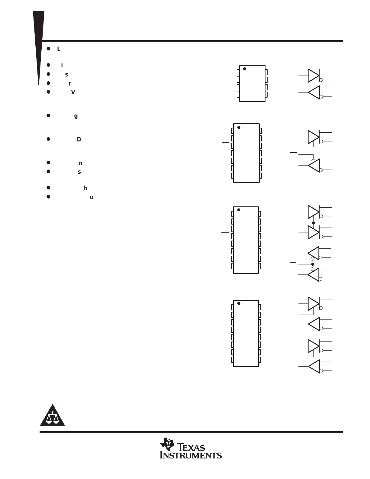
SN65LVDM179D (Marked as DM179 or LVM179)
SN65LVDM179DGK (Marked as M79)
SN65LVDM180D (Marked as LVDM180)
GND
GND
SN65LVDM050D (Marked as LVDM050)
GND
SN65LVDM051D (Marked as LVDM051)
1DE
GND
V
CC
GND
NC
R
RE
DE
D
1B
1A
1R
RE
2R
2A
2B
1B
1A
1R
2R
2A
2B
R
D
(TOP VIEW)
1
2
3
4
(TOP VIEW)
1
14
2
13
3
12
4
11
5
10
6
7
(TOP VIEW)
1
16
2
15
3
14
4
13
5
12
6
11
7
10
8
(TOP VIEW)
1
16
2
15
3
14
4
13
5
12
6
11
7
10
8
A
8
B
7
Z
6
5
Y
V
CC
V
CC
A
B
D
R
D
DE
RE
Z
1D
DE
2D
R
15
12
Y
9
NC
8
V
CC
1D
1Y
1Z
DE
2Z
1R
2Y
9
2D
V
CC
1D
1Y
1Z
RE
2R
1D
1DE
1R
15
2DE
2Z
2Y
9
2D
2D
2DE
2R
12
3
2
5
4
3
2
9
3
4
5
4
3
9
5
5
Y
6
Z
8
A
7
B
9
Y
10
Z
12
A
11
B
14
1Y
13
1Z
10
2Y
11
2Z
2
1A
1
1B
6
2A
7
2B
14
1Y
13
1Z
2
1A
1
1B
10
2Y
11
2Z
6
2A
7
2B
Please be aware that an important notice concerning availability, standard warranty, and use in critical applications of
Texas Instruments semiconductor products and disclaimers thereto appears at the end of this data sheet.
PRODUCTION DATA information is current as of publication date.
Products conform to specifications per the terms of Texas Instruments
standard warranty. Production processing does not necessarily include
testing of all parameters.
POST OFFICE BOX 655303 • DALLAS, TEXAS 75265
Copyright 1998, Texas Instruments Incorporated
1
SN65LVDM179, SN65LVDM180, SN65LVDM050, SN65LVDM051
40°C to 85°C
HIGH-SPEED DIFFERENTIAL LINE DRIVERS AND RECEIVERS
SLLS324B – DECEMBER 1998 – REVISED MARCH 2000
description (continued)
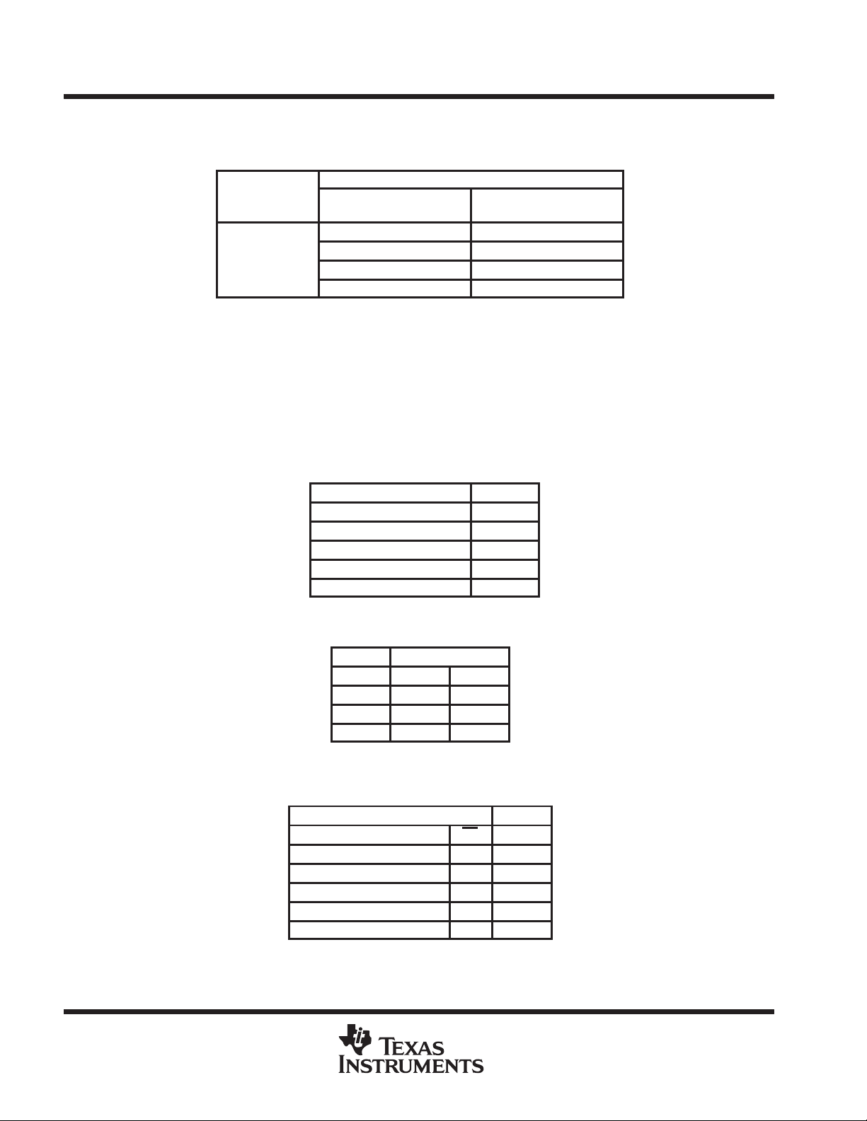
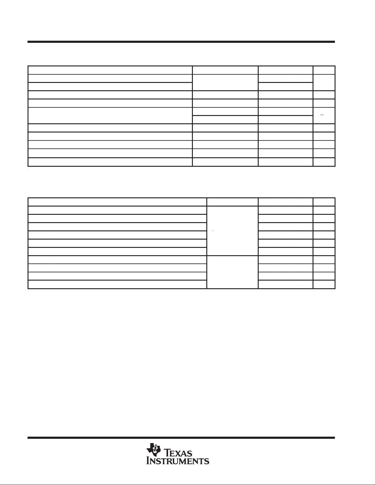
AVAILABLE OPTIONS
PACKAGE
T
A
°
–
°
The ultimate rate and distance of data transfer is dependent upon the attenuation
characteristics of the media, the noise coupling to the environment, and other application
specific characteristics.
The SN65LVDM179, SN65LVDM180, SN65LVDM050, and SN65LVDM051 are characterized for operation
from –40°C to 85°C.
SMALL OUTLINE
(D)
SN65LVDM050D —
SN65LVDM051D —
SN65LVDM179D SN65LVDM179DGK
SN65LVDM180D —
SMALL OUTLINE
(DGK)
NOTE:
Function Tables
SN65LVDM179 RECEIVER
INPUTS
VID = VA – V
VID ≥ 100 mV H
–100 MV < VID < 100 mV ?
VID ≤ –100 mV L
Open H
H = high level, L = low level, ? = indeterminate
SN65LVDM179 DRIVER
INPUT
D Y Z
L L H
H H L
Open L H
H = high level, L = low level
SN65LVDM180, SN65LVDM050, and
SN65LVDM051 RECEIVER
INPUTS
VID = VA – V
VID ≥ 100 mV L H
–100 MV < VID < 100 mV L ?
VID ≤ –100 mV L L
Open L H
X H Z
H = high level, L = low level, Z = high impedance,
X = don’t care
B
OUTPUTS
B
OUTPUT
R
OUTPUT
RE R
2
POST OFFICE BOX 655303 • DALLAS, TEXAS 75265

SN65LVDM179, SN65LVDM180, SN65LVDM050, SN65LVDM051
HIGH-SPEED DIFFERENTIAL LINE DRIVERS AND RECEIVERS
SN65LVDM180, SN65LVDM050, and
SN65LVDM051 DRIVER
INPUTS OUTPUTS
D DE Y Z
L H L H
H H H L
Open H L H
X L Z Z
H = high level, L = low level, Z = high impedance,
X = don’t care
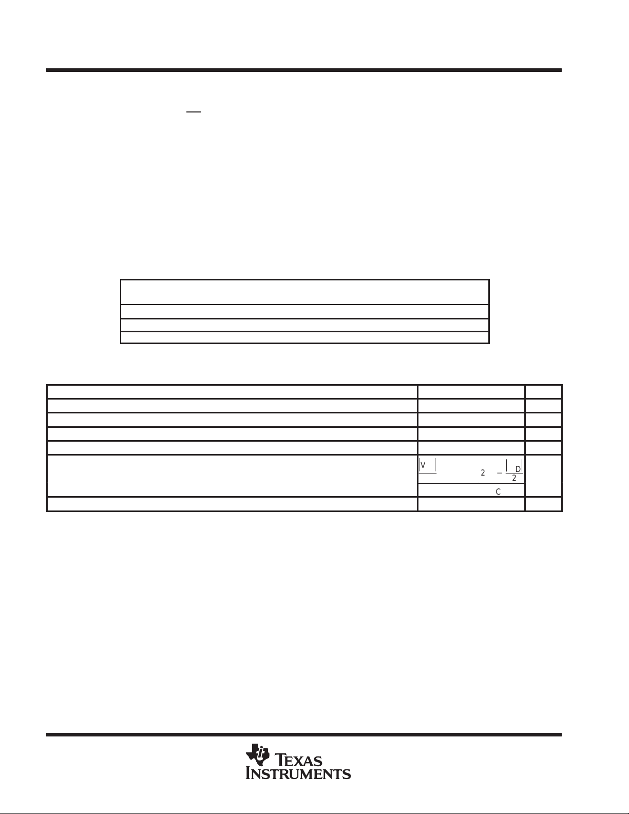
equivalent input and output schematic diagrams
V
CC
300 kΩ
D or RE
Input
7 V
50 Ω
300 kΩ
DE
50 Ω
Input
7 V
SLLS324B – DECEMBER 1998 – REVISED MARCH 2000
V
CC
V
CC
10 kΩ
5 Ω
Y or Z
Output
7 V
7 V
V
CC
300 kΩ300 kΩ
B InputA Input
7 V
V
CC
5 Ω
R Output
7 V
POST OFFICE BOX 655303 • DALLAS, TEXAS 75265
3
SN65LVDM179, SN65LVDM180, SN65LVDM050, SN65LVDM051
HIGH-SPEED DIFFERENTIAL LINE DRIVERS AND RECEIVERS
SLLS324B – DECEMBER 1998 – REVISED MARCH 2000
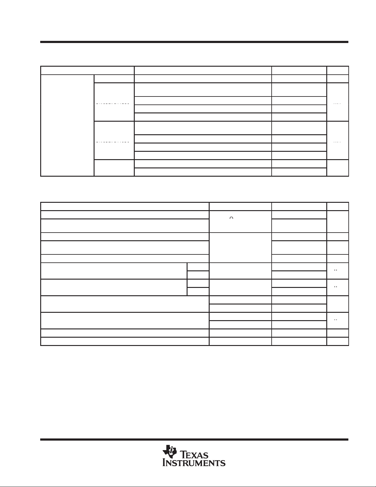
absolute maximum ratings over operating free-air temperature (unless otherwise noted)
†
Supply voltage range, VCC (see Note 1) –0.5 V to 4 V. . . . . . . . . . . . . . . . . . . . . . . . . . . . . . . . . . . . . . . . . . . . . .
Voltage range (D, R, DE, RE) –0.5 V to 6 V. . . . . . . . . . . . . . . . . . . . . . . . . . . . . . . . . . . . . . . . . . . . . . . . . . . . . . . .
Voltage range (Y, Z, A, and B) –0.5 V to 4 V. . . . . . . . . . . . . . . . . . . . . . . . . . . . . . . . . . . . . . . . . . . . . . . . . . . . . . .
Electrostatic discharge (Y, Z, A, B , and GND) (see Note 2) CLass 3, A:12 kV, B:600 V. . . . . . . . . . . . . . . . . .
All Class 3, A:7 kV, B:500 V. . . . . . . . . . . . . . . . . . . . . . . . . . . . . . . . . . . . . . . . . . . . . . . .
Continuous power dissipation see dissipation rating table. . . . . . . . . . . . . . . . . . . . . . . . . . . . . . . . . . . . . . . . . . .
Storage temperature range –65°C to 150°C. . . . . . . . . . . . . . . . . . . . . . . . . . . . . . . . . . . . . . . . . . . . . . . . . . . . . . . .
Lead temperature 1,6 mm (1/16 inch) from case for 10 seconds 250°C. . . . . . . . . . . . . . . . . . . . . . . . . . . . . . .
†
Stresses beyond those listed under “absolute maximum ratings” may cause permanent damage to the device. These are stress ratings only, and
functional operation of the device at these or any other conditions beyond those indicated under “recommended operating conditions” is not
implied. Exposure to absolute-maximum-rated conditions for extended periods may affect device reliability.
NOTES: 1. All voltage values, except differential I/O bus voltages are with respect to network ground terminal.
2. Tested in accordance with MIL-STD-883C Method 3015.7.
DISSIPATION RATING TABLE
PACKAGE
D8 725 mW 5.8 mW/°C 377 mW
D14 or D16 950 mW 7.8 mW/°C 494 mW
DGK 424 mW 3.4 mW/°C 220 mW
†
This is the inverse of the junction-to-ambient thermal resistance when board-mounted and with no air flow.
TA ≤ 25°C
POWER RATING
DERATING FACTOR
ABOVE TA = 25°C
†
TA = 85°C
POWER RATING
recommended operating conditions
MIN NOM MAX UNIT
Supply voltage, V
High-level input voltage, V
Low-level input voltage, V
Magnitude of differential input voltage, VID 0.1 0.6 V
Common–mode input voltage, VIC (see Figure 6)
Operating free–air temperature, T
CC
IH
IL
A
3 3.3 3.6 V
2 V
0.8 V
Ť
Ť
V
ID
2
–40 85 °C
2.4
*
VCC–0.8
Ť
V
ID
2
Ť
V
4
POST OFFICE BOX 655303 • DALLAS, TEXAS 75265
SN65LVDM180
mA
SN65LVDM050
mA
SN65LVDM051
mA
R
IIHHigh-level input current
V
5 V
A
IILLow-level input current
V
V
A
IOSShort-circuit output current
mA
IOZHigh-impedance output current
A
SN65LVDM179, SN65LVDM180, SN65LVDM050, SN65LVDM051
HIGH-SPEED DIFFERENTIAL LINE DRIVERS AND RECEIVERS
SLLS324B – DECEMBER 1998 – REVISED MARCH 2000
device electrical characteristics over recommended operating conditions (unless otherwise
noted)
PARAMETER TEST CONDITIONS MIN TYP†MAX UNIT
SN65LVDM179 No receiver load, Driver RL = 50 Ω 10 15 mA
Driver and receiver enabled, No receiver load,
Driver RL = 50 Ω
SN65LVDM180
I
Supply current
CC
SN65LVDM050
†
All typical values are at 25°C and with a 3.3 V supply.
Driver enabled, Receiver disabled, RL = 50 Ω 9 13
Driver disabled, Receiver enabled, No load 1.7 5
Disabled 0.5 2
Drivers and receivers enabled, No receiver loads,
Driver RL = 50 Ω
Drivers enabled, Receivers disabled, RL = 50 Ω 16 24
Drivers disabled, Receivers enabled, No loads 4 6
Disabled 0.5 1
Drivers enabled, No receiver loads, Driver RL = 50 Ω 19 27
Drivers disabled, No loads 4 6
10 15
mA
19 27
mA
driver electrical characteristics over recommended operating conditions (unless otherwise noted)
PARAMETER TEST CONDITIONS MIN TYP MAX UNIT
VOD Differential output voltage magnitude
∆VOD
V
OC(SS)
∆V
OC(SS)
V
OC(PP)
I
O(OFF)
C
IN
Change in differential output voltage magnitude between logic
states
Steady-state common-mode output voltage 1.125 1.2 1.375 V
Change in steady-state common-mode output voltage between
logic states
Peak-to-peak common-mode output voltage 50 150 mV
p
p
p
p
Power-off output current VCC = 0 V, VO = 3.6 V ±1 µA
Input capacitance 3 pF
p
= 50 Ω,
L
See Figure 1 and Figure 2
See Figure 3
DE
D
DE
D
=
IH
= 0.8
IL
VOY or VOZ = 0 V 7 10
VOD = 0 V 7 10
VOD = 600 mV ±1
VO = 0 V or V
CC
247 340 454
±1
mV
µ
µ
µ
–50 50
–50 50 mV
–0.5 –20
2 20
–0.5 –10
2 10
POST OFFICE BOX 655303 • DALLAS, TEXAS 75265
5
SN65LVDM179, SN65LVDM180, SN65LVDM050, SN65LVDM051
See Figure 5 and Table 1
mV
IIInput current (A or B inputs)
A
C
See
6
See Figure 6
See Figure 7
HIGH-SPEED DIFFERENTIAL LINE DRIVERS AND RECEIVERS
SLLS324B – DECEMBER 1998 – REVISED MARCH 2000
receiver electrical characteristics over recommended operating conditions (unless otherwise
noted)
PARAMETER TEST CONDITIONS MIN TYP†MAX UNIT
V
ITH+
V
ITH–
V
OH
V
OL
I
I(OFF)
I
IH
I
IL
I
OZ
C
I
†
All typical values are at 25°C and with a 3.3-V supply.
driver switching characteristics over recommended operating conditions (unless otherwise
noted)
t
PLH
t
PHL
t
r
t
f
t
sk(p)
t
sk(o)
t
PZH
t
PZL
t
PHZ
t
pLZ
†
All typical values are at 25°C and with a 3.3-V supply.
‡
t
sk(o)
Positive-going differential input voltage threshold
Negative-going differential input voltage threshold
High-level output voltage IOH = –8 mA 2.4 V
Low-level output voltage IOL = 8 mA 0.4 V
p
Power-off input current (A or B inputs) VCC = 0 ±20 µA
High-level input current (enables) VIH = 5 V 10 µA
Low-level input current (enables) VIL = 0.8 V 10 µA
High-impedance output current VO = 0 or 5 V ±10 µA
Input capacitance 5 pF
Propagation delay time, low-to-high-level output 1.7 2.7 ns
Propagation delay time, high-to-low-level output 1.7 2.7 ns
Differential output signal rise time
Differential output signal fall time
Pulse skew (|t
Channel-to-channel output skew
Propagation delay time, high-impedance-to-high-level output 6 10 ns
Propagation delay time, high-impedance-to-low-level output
Propagation delay time, high-level-to-high-impedance output
Propagation delay time, low-level-to-high-impedance output 5 10 ns
is the maximum delay time difference between drivers on the same device.
p
PARAMETER TEST CONDITIONS MIN TYP†MAX UNIT
– t
pLH
|)
‡
pHL
VI = 0 –2 –11 –20
VI = 2.4 V –1.2 –3
RL = 50Ω,
= 10 pF,
p
L
Figure
–100
250 ps
100 ps
100
0.6 1 ns
0.6 1 ns
6 10 ns
4 10 ns
µ
6
POST OFFICE BOX 655303 • DALLAS, TEXAS 75265
 Loading...