


SN65LBC179D
Texas Instruments SN65LBC179D, SN65LBC179DR, SN65LBC179P, SN65LBC179QD, SN65LBC179QDR Datasheet
...
SN75LBC179, SN65LBC179, SN65LBC179Q
LOW-POWER DIFFERENTIAL LINE DRIVER AND RECEIVER PAIRS
SLLS173C – JANUARY 1994 – REVISED JANUARY 2000
1
POST OFFICE BOX 655303 • DALLAS, TEXAS 75265
D
Designed for High-Speed Multipoint Data
Transmission Over Long Cables
D
Operate With Pulse Widths as Low
as 30 ns
D
Low Supply Current ...5 mA Max
D
Meets or Exceeds the Standard
Requirements of ANSI RS-485 and
ISO 8482:1987(E)
D
Common-Mode Voltage Range of –7 V
to 12 V
D
Positive- and Negative-Output Current
Limiting
D
Driver Thermal Shutdown Protection
D
Pin Compatible With the SN75179B
description
The SN65LBC179, SN65LBC179Q, and
SN75LBC179 differential driver and receiver pairs
are monolithic integrated circuits designed for
bidirectional data communication over long
cables that take on the characteristics of
transmission lines. They are balanced, or
differential, voltage mode devices that meet or
exceed the requirements of industry standards
ANSI RS-485 and ISO 8482:1987(E). Both
devices are designed using TI’s proprietary
LinBiCMOS with the low power consumption of
CMOS and the precision and robustness of
bipolar transistors in the same circuit.
The SN65LBC179, SN65LBC179Q, and
SN75LBC179 combine a differential line driver
and differential line receiver and operate from a
single 5-V supply. The driver differential outputs
and the receiver differential inputs are connected
to separate terminals for full-duplex operation and
are designed to present minimum loading to the
bus when powered off (V
CC
= 0). These parts
feature a wide common-mode voltage range
making them suitable for point-to-point or
multipoint data bus applications. The devices also
provide positive- and negative-current limiting
and thermal shutdown for protection from line fault
conditions. The line driver shuts down at a junction
temperature of approximately 172°C.
Copyright 2000, Texas Instruments Incorporated
PRODUCTION DATA information is current as of publication date.
Products conform to specifications per the terms of Texas Instruments
standard warranty. Production processing does not necessarily include
testing of all parameters.
Please be aware that an important notice concerning availability, standard warranty, and use in critical applications of
Texas Instruments semiconductor products and disclaimers thereto appears at the end of this data sheet.
LinBiCMOS is a trademark of Texas Instruments Incorporated.
logic symbol
†
logic diagram (positive logic)
Y
Z
B
A
R
D
5
6
7
8
2
3
R
D
B
A
Z
Y
7
8
6
5
2
3
†
This symbol is in accordance with ANSI/IEEE Std 91-1984
and IEC Publication 617-12.
INPUT
D
OUTPUTS
Y Z
DRIVER
DIFFERENTIAL INPUTS
A–B
VID ≥ 0.2 V
–0.2 V < VID < 0.2 V
VID ≤ – 0.2 V
Open circuit
OUTPUT
R
H
?
L
H
RECEIVER
H = high level, L = low level,
? = indeterminate
Function Tables
1
2
3
4
8
7
6
5
V
CC
R
D
GND
A
B
Z
Y
D OR P PACKAGE
(TOP VIEW)
H
L
HLL
H
SN75LBC179, SN65LBC179, SN65LBC179Q
LOW-POWER DIFFERENTIAL LINE DRIVER AND RECEIVER PAIRS
SLLS173C – JANUARY 1994 – REVISED JANUARY 2000
2
POST OFFICE BOX 655303 • DALLAS, TEXAS 75265
description (continued)
The SN65LBC179, SN65LBC179Q, and SN75LBC179 are available in the 8-pin dual-in-line and small-outline
packages. The SN75LBC179 is characterized for operation over the commercial temperature range of 0°C to
70°C. The SN65LBC179 is characterized over the industrial temperature range of –40°C to 85°C. The
SN65LBC179Q is characterized over the extended industrial or automotive temperature range of – 40°C to
125°C.
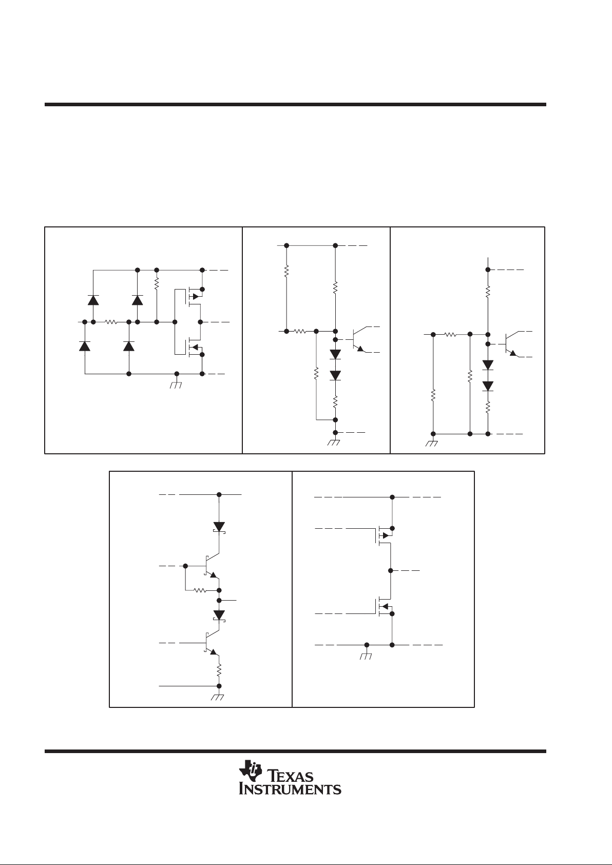
schematics of inputs and outputs
RECEIVER A INPUTEQUIVALENT OF DRIVER INPUT RECEIVER B INPUT
DRIVER OUTPUT TYPICAL OF RECEIVER OUTPUT
Output
V
CC
V
CC
100 kΩ
NOM
3 kΩ
NOM
Input
18 kΩ
NOM
1.1 kΩ
NOM
1.1 kΩ
NOM
3 kΩ
NOM
18 kΩ
NOM
100 kΩ
NOM
Input
V
CC
Input
V
CC
22 kΩ
V
CC
R Output
12 kΩ
12 kΩ
SN75LBC179, SN65LBC179, SN65LBC179Q
LOW-POWER DIFFERENTIAL LINE DRIVER AND RECEIVER PAIRS
SLLS173C – JANUARY 1994 – REVISED JANUARY 2000
3
POST OFFICE BOX 655303 • DALLAS, TEXAS 75265
absolute maximum ratings over operating free-air temperature range (unless otherwise noted)
†
Supply voltage range, VCC –0.3 V to 7 V. . . . . . . . . . . . . . . . . . . . . . . . . . . . . . . . . . . . . . . . . . . . . . . . . . . . . . . . . .
Voltage range at A, B, Y, or Z (see Note 1) –10 V to 15 V. . . . . . . . . . . . . . . . . . . . . . . . . . . . . . . . . . . . . . . . . . . .
Voltage range at D or R (see Note 1) –0.3 V to VCC + 0.5 V. . . . . . . . . . . . . . . . . . . . . . . . . . . . . . . . . . . . . . . . .
Continuous total power dissipation (see Note 2) Internally limited. . . . . . . . . . . . . . . . . . . . . . . . . . . . . . . . . . . . . .
Total power dissipation See Dissipation Rating Table. . . . . . . . . . . . . . . . . . . . . . . . . . . . . . . . . . . . . . . . . . . . . . .
Operating free-air temperature range, T
A
: SN65LBC179 –40°C to 85°C. . . . . . . . . . . . . . . . . . . . . . . . . . . . . . .
SN65LBC179Q –40°C to 125°C. . . . . . . . . . . . . . . . . . . . . . . . . . . .
SN75LBC179 0°C to 70°C. . . . . . . . . . . . . . . . . . . . . . . . . . . . . . . . .
Storage temperature range, T
stg
–65°C to 150°C. . . . . . . . . . . . . . . . . . . . . . . . . . . . . . . . . . . . . . . . . . . . . . . . . . .
Lead temperature 1,6 mm (1/16 inch) from case for 10 seconds 260°C. . . . . . . . . . . . . . . . . . . . . . . . . . . . . . .
†
Stresses beyond those listed under “absolute maximum ratings” may cause permanent damage to the device. These are stress ratings only, and
functional operation of the device at these or any other conditions beyond those indicated under “recommended operating conditions” is not
implied. Exposure to absolute-maximum-rated conditions for extended periods may affect device reliability.
NOTES: 1. All voltage values are with respect to GND.
2. The maximum operating junction temperature is internally limited. Uses the dissipation rating table to operate below this
temperature.
DISSIPATION RA TING TABLE
PACKAGE
TA ≤ 25°C
POWER RATING
DERATING FACTOR
ABOVE TA = 25°C
TA = 70°C
POWER RATING
TA = 85°C
POWER RATING
D 725 mW 5.8 mW/°C 464 mW 377 mW
P 1100 mW 8.8 mW/°C 704 mW 572 mW
recommended operating conditions
MIN NOM MAX UNIT
Supply voltage, V
CC
4.75 5 5.25 V
High-level input voltage, V
IH
D 2 V
Low-level input voltage, V
IL
D 0.8 V
Differential input voltage, V
ID
–6
‡
6 V
Voltage at any bus terminal (separately or common-mode), VO, VI, or V
IC
A, B, Y, or Z –7 12 V
p
Y or Z –60
High-level output current, I
OH
R –8
mA
p
Y or Z 60
Low-level output current, I
OL
R 8
mA
SN65LBC179 –40 85
Operating free-air temperature, T
A
SN65LBC179Q –40 125
°C
SN75LBC179 0 70
‡
The algebraic convention, in which the least positive (most negative) limit is designated as minimum, is used in this data sheet for differential
input voltage, voltage at any bus terminal (separately or common mode), operating temperature, input threshold voltage, and common-mode
output voltage.
SN75LBC179, SN65LBC179, SN65LBC179Q
LOW-POWER DIFFERENTIAL LINE DRIVER AND RECEIVER PAIRS
SLLS173C – JANUARY 1994 – REVISED JANUARY 2000
4
POST OFFICE BOX 655303 • DALLAS, TEXAS 75265
DRIVER SECTION
electrical characteristics over recommended operating conditions (unless otherwise noted)
PARAMETER TEST CONDITIONS MIN TYP†MAX UNIT
V
IK
Input clamp voltage II = –18 mA –1.5 V
RL = 54 Ω,
SN65LBC179,
SN65LBC179Q
1.1 2.2 5
p
See Figure 1
SN75LBC179 1.5 2.2 5
|VOD|
Differential output voltage (see Note 3)
RL = 60 Ω,
SN65LBC179,
SN65LBC179Q
1.1 2.2 5
V
See Figure 2
SN75LBC179 1.5 2.2 5
∆|VOD|
Change in magnitude of differential
output voltage (see Note 4)
See Figures 1 and 2 ±0.2 V
V
OC
Common-mode output voltage 1 2.5 3 V
∆|VOC|
Change in magnitude of common-mode output
voltage (see Note 4)
RL = 54 Ω, See Figure 1
±0.2 V
I
O
Output current with power off VCC = 0, VO = –7 V to 12 V ±100 µA
I
IH
High-level input current VI = 2.4 V –100 µA
I
IL
Low-level input current VI = 0.4 V –100 µA
I
OS
Short-circuit output current –7 V ≤ VO ≤ 12 V ±250 mA
I
CC
Supply current No load
SN65LBC179,
SN75LBC179
4.2 5 mA
CC
y
SN65LBC179Q 4.2 7 mA
†
All typical values are at VCC = 5 V and TA = 25°C.
NOTES: 3. The minimum VOD specification of the SN65179 may not fully comply with ANSI RS-485 at operating temperatures below 0°C.
System designers should take the possibly lower output signal into account in determining the maximum signal transmission
distance.
4. ∆|VOD| and ∆|VOC| are the changes in the steady-state magnitude of VOD and VOC, respectively, that occur when the input is
changed from a high level to a low level.
switching characteristics, VCC = 5 V, TA = 25°C
PARAMETER TEST CONDITIONS MIN MAX UNIT
t
d(OD)
Differential-output delay time
7 18 ns
t
t(OD)
Differential transition time
R
L
= 54 Ω,
See Figure 3
5 20 ns
 Loading...