Analog Devices AD7118UQ, AD7118TQ, AD7118LN, AD7118KN, AD7118CQ Datasheet

a |
LOGDAC |
|
CMOS Logarithmic D/A Converter |
||
|
|
AD7118* |
|
|
|
FEATURES
Dynamic Range 85.5 dB Resolution 1.5 dB
Full 625 V Input Range Multiplying DAC
Full Military Temperature Range –558C to +1258C
Low Distortion
Low Power Consumption
Latch Proof Operation (Schottky Diodes Not Required) Single 5 V to 15 V Supply
APPLICATIONS
Digitally Controlled AGC Systems
Audio Attenuators
Wide Dynamic Range A/D Converters
Sonar Systems
Function Generators
GENERAL DESCRIPTION
The LOGDAC® AD7118 is a CMOS multiplying D/A converter which attenuates an analog input signal over the range
0 to –85.5 dB in 1.5 dB steps. The analog output is determined by a six-bit attenuation code applied to the digital inputs. Operating frequency range of the device is from dc to several hundred kHz.
The device is manufactured using an advanced monolithic silicon gate thin-film on CMOS process and is packaged in a 14-pin dual-in-line package.
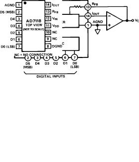
FUNCTIONAL DIAGRAM
PIN CONFIGURATION
ORDERING INFORMATION
|
|
Specified |
|
|
Temperature |
Accuracy |
Package |
Model |
Range |
Range |
Option1 |
AD7118KN |
0°C to +70°C |
0 to 42 dB |
N-16 |
AD7118LN |
0°C to +70°C |
0 to 48 dB |
N-16 |
AD7118BQ |
–25°C to +85°C |
0 to 42 dB |
Q-16 |
AD7118CQ |
–25°C to +85°C |
0 to 48 dB |
Q-16 |
AD7118TQ2 |
–55°C to +125°C |
0 to 42 dB |
Q-16 |
AD7118UQ2 |
–55°C to +125°C |
0 to 48 dB |
Q-16 |
NOTES
1N = Plastic DIP; Q = Cerdip.
2To order MIL-STD-883, Class B processed parts, add /883B to part number.
*Protected by U.S. Patent No. 4521,764.
LOGDAC is a registered trademark of Analog Devices, Inc.
REV. A
Information furnished by Analog Devices is believed to be accurate and reliable. However, no responsibility is assumed by Analog Devices for its use, nor for any infringements of patents or other rights of third parties which may result from its use. No license is granted by implication or otherwise under any patent or patent rights of Analog Devices.
One Technology Way, P.O. Box 9106, Norwood, MA 02062-9106, U.S.A. Tel: 617/329-4700 Fax: 617/326-8703

AD7118–SPECIFICATIONS |
(VDD = +5 V or +15 V, VIN = –10 V dc, IOUT = AGND = DGND = 0 V, output amplifier |
||||||||||
AD544 except where noted) |
|
|
|
||||||||
|
|
TA = +258C |
TA = TMIN, TMAX |
|
|
||||||
Parameter |
|
VDD = +5 V |
|
VDD = +15 V |
VDD = +5 V |
|
VDD = +15 V |
Units |
Test Conditions/Comments |
||
NOMINAL RESOLUTION |
|
1.5 |
|
1.5 |
|
1.5 |
|
1.5 |
dB |
|
|
|
|
|
|
|
|
|
|
|
|
||
ACCURACY RELATIVE TO VIN |
|
|
|
|
|
|
|
|
|
||
AD7118L/C/U |
|
±0.35 |
|
±0.35 |
±0.4 |
|
±0.4 |
|
|
||
0 dB to –30 dB |
|
|
|
dB max |
Accuracy is measured using |
||||||
–31.5 dB to –42 dB |
|
±0.7 |
|
±0.5 |
|
±0.8 |
|
±0.7 |
dB max |
circuit of Figure 1 and includes |
|
–43.5 dB to –48 dB |
|
±1.0 |
|
±0.7 |
|
±1.3 |
|
±1.0 |
dB max |
any effects due to mismatch |
|
AD7118K/B/T |
|
±0.5 |
|
±0.5 |
|
±0.5 |
|
±0.5 |
|
between RFB and the R-2R |
|
0 dB to –30 dB |
|
|
|
|
dB max |
ladder circuit. |
|||||
–31.5 dB to –42 dB |
|
±0.75 |
|
±0.75 |
±1.0 |
|
±0.8 |
dB max |
|
||
MONOTONIC RANGE |
|
|
|
|
|
|
|
|
|
|
|
Nominal 1.5 dB Steps |
L/C/U Grade |
Monotonic Over Full |
0 to –72 |
|
0 to –72 |
dB |
Digital Inputs 000000 to 110000 |
||||
|
K/B/T Grade |
Code Range |
|
|
|
0 to –66 |
|
0 to –66 |
dB |
Digital Inputs 000000 to 101100 |
|
|
|
|
|
|
|||||||
Nominal 3 dB Steps |
All Grades |
Monotonic Over Full Code Range |
|
|
|
|
|||||
VIN INPUT RESISTANCE |
All Grades |
9 |
|
9 |
|
9 |
|
9 |
kW min |
|
|
(PIN 12) |
L/C/U Grade |
17 |
|
17 |
|
17 |
|
17 |
kW max |
|
|
|
K/B/T Grade |
21 |
|
21 |
|
21 |
|
21 |
kW max |
|
|
RFB INPUT RESISTANCE |
All Grades |
9.45 |
|
9.45 |
|
9.45 |
|
9.45 |
kW min |
|
|
(PIN 13) |
L/C/U Grade |
18 |
|
18 |
|
18 |
|
18 |
kW max |
|
|
|
K/B/T Grade |
22 |
|
22 |
|
22 |
|
22 |
kW max |
|
|
DIGITAL INPUTS |
|
|
|
|
|
|
|
|
|
|
|
Input High Voltage Requirements VIH |
3.0 |
|
13.5 |
|
3.0 |
|
13.5 |
V min |
|
||
Input Low Voltage Requirements VIL |
0.8 |
|
1.5 |
|
0.8 |
|
1.5 |
V max |
|
||
Input Leakage Current |
|
±1 |
|
±1 |
|
±10 |
|
±10 |
mA max |
Digital Inputs = VDD |
|
POWER SUPPLY |
|
|
|
|
|
|
|
|
|
|
|
VDD for Specified Accuracy |
|
5 |
|
– |
|
5 |
|
– |
V min |
|
|
|
|
– |
|
15 |
|
– |
|
15 |
V max |
|
|
IDD |
|
0.5 |
|
1 |
|
1 |
|
2 |
mA max |
Digital Inputs = 0 V or VDD |
|
|
|
|
|
|
|
|
|
|
|
(See Figure 7) |
|
|
|
|
|
|
|
|
|
|
|
|
|
Specifications subject to change without notice. |
|
|
|
(VDD = +5 V or +15 V, VIN = –10 V except where stated, IOUT = AGND = DGND = |
|||||||
AC PERFORMANCE CHARACTERISTICS |
|||||||||||
0 V, output amplifier AD544 except where noted) |
|||||||||||
These characteristics are included for design guidance only and are not subject to test.
|
|
TA = +258C |
TA = TMIN, TMAX |
|
|
|
|
||
Parameter |
|
VDD = +5 V |
VDD = +15 V |
VDD = +5 V |
VDD = +15 V |
Units |
|
||
DC Supply Rejection, DGain/DVDD |
0.01 |
0.005 |
0.01 |
0.005 |
dB per % max |
DVDD = ±10%, |
|||
|
|
|
|
|
|
ms max |
Input code = 100000 |
||
Propagation Delay |
|
1.8 |
0.4 |
2.2 |
0.5 |
Full-Scale Change |
|||
Digital-to-Analog Glitch Impulse |
225 |
1200 |
– |
– |
nV secs typ |
Measured with ADLH0032CG |
|||
|
|
|
|
|
|
|
|
|
as output amplifier for input |
|
|
|
|
|
|
|
|
|
code transition 100000 to 000000. |
|
|
|
|
|
|
|
|
|
C1 of Figure 1 is 0 pF. |
Output Capacitance (Pin 14) |
|
100 |
100 |
100 |
100 |
pF max |
|
||
Input Capacitance Pin 12 and Pin 13 |
7 |
7 |
7 |
7 |
pF max |
|
|||
Feedthrough at 1 kHz |
L/C/U Grade |
–86 |
–86 |
–68 |
–68 |
dB max |
Feedthrough is also deter- |
||
|
K/B/T Grade |
–80 |
–80 |
–63 |
–63 |
dB max |
mined by circuit layout |
||
Total Harmonic Distortion |
|
–85 |
–85 |
–85 |
–85 |
dB typ |
VIN = 6 V rms |
||
Intermodulation Distortion |
|
–79 |
–79 |
–79 |
–79 |
dB typ |
per DIN 45403 Blatt 4 |
||
Output Noise Voltage Density |
70 |
70 |
70 |
70 |
nV/Ö |
Hz |
max |
Includes AD544 amplifier noise |
|
Digital Input Capacitance |
|
7 |
7 |
7 |
7 |
pF max |
|
||
|
|
|
|
|
|
|
|
|
|
Specifications subject to change without notice.
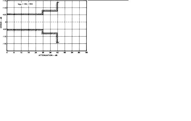
Accuracy Specification for K/B/T Grade Devices at TA = +25°C |
Accuracy Specification for L/C/U Grade Devices at TA = +25°C |
–2– |
REV. A |
 Loading...