


AD688SQ
Table of contents
 Loading...
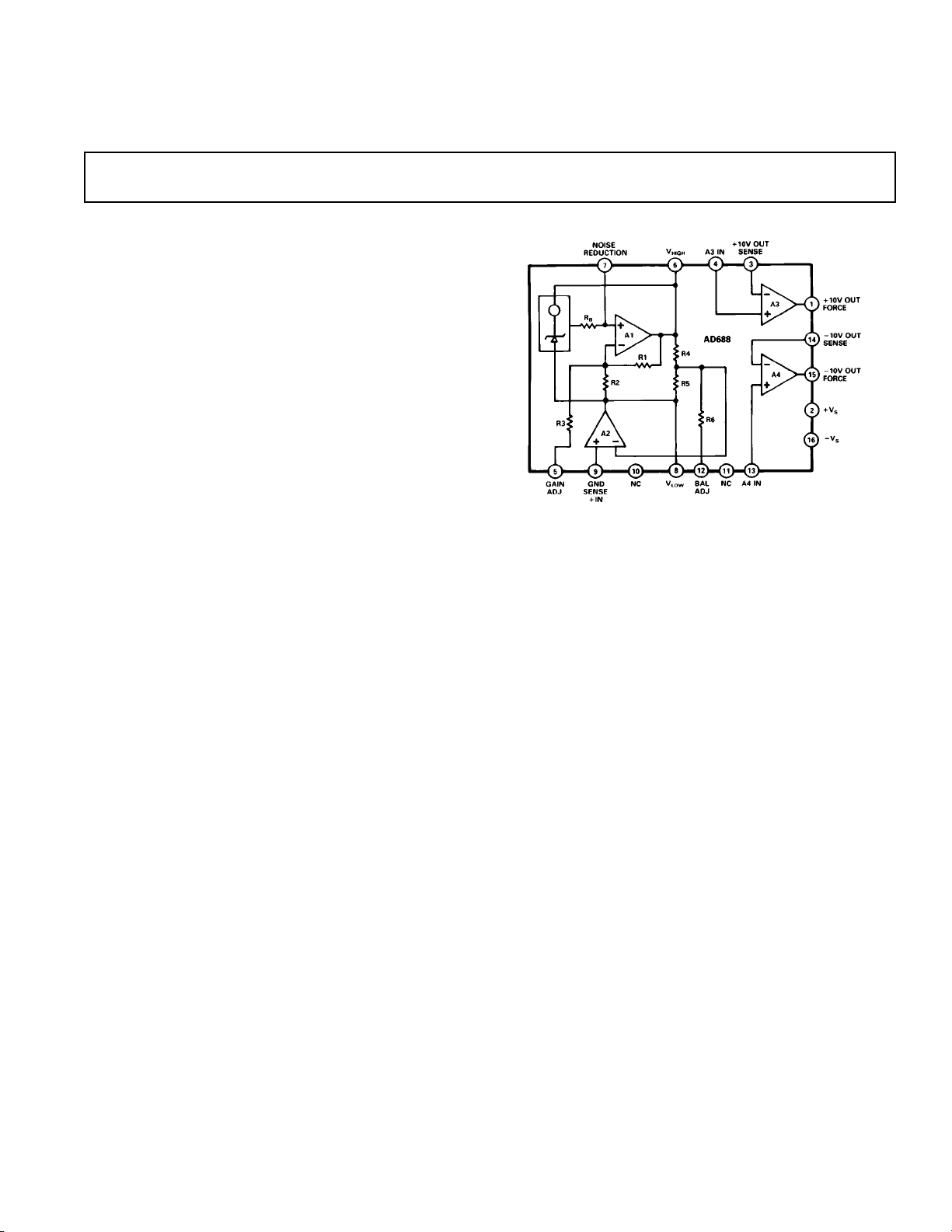
High Precision
a
FEATURES 610 V Tracking Outputs Kelvin Connections Low Tracking Error – 1.5 mV Low Initial Error – 2.0 mV Low Drift – 1.5 ppm/8C Low Noise – 6 mV p-p Flexible Output Force and Sense Terminals High Impedance Ground Sense Machine Insertable DIP Packaging MIL-STD-883 Compliant Versions Available
PRODUCT DESCRIPTION
The AD688 is a high precision ±10 V tracking reference. Low
tracking error, low initial error and low temperature drift give
the AD688 reference absolute ±10 V accuracy performance
previously unavailable in monolithic form. The AD688 uses a
proprietary ion-implanted buried Zener diode, and laser-waferdrift-trimming of high stability thin-film resistors to provide
outstanding performance at low cost.
The AD688 includes the basic reference cell and three additional
amplifiers. The amplifiers are laser-trimmed for low offset and
low drift and maintain the accuracy of the reference. The
amplifiers are configured to allow Kelvin connections to the
load and/or boosters for driving long lines or high current loads,
delivering the full accuracy of the AD688 where it is required in
the application circuit.
The low initial error allows the AD688 to be used as a system
reference in precision measurement applications requiring
12-bit absolute accuracy. In such systems, the AD688 can
provide a known voltage for system calibration and the cost of
periodic recalibration can therefore be eliminated. Furthermore,
the mechanical instability of a trimming potentiometer and the
potential for improper calibration can be eliminated by using
the AD688 and calibration software.
The AD688 is available in three versions. The AD688AQ and
BQ grades are packaged in 16-pin cerdip (0.3") packages and
are specified for operation from –40°C to +85°C. The AD688SQ
grade is specified for operation from –55°C to +125°C.
610 V Reference
AD688*
FUNCTIONAL BLOCK DIAGRAM
PRODUCT HIGHLIGHTS
1. The AD688 offers precision tracking ± 10 V Kelvin output
connections with no external components. Tracking error is
less than 1.5 mV and a fine-trim is available for applications
requiring exact symmetry between the +10 V and –10 V
outputs.
2. The AD688 offers 12-bit absolute accuracy without any user
adjustments. Optional fine-trim connections are provided for
applications requiring higher precision. The fine-trimming
does not alter the operating conditions of the Zener or the
buffer amplifiers and thus does not increase the temperature
drift.
3. Output noise of the AD688 is low – typically 6 µV p-p. A pin
is provided for broadband noise filtering using an external
capacitor.
4. The AD688 is available in versions compliant with MILSTD-883. Refer to the Analog Devices Military Products
Databook or current AD688/883B data sheet for detailed
specifications.
*Covered by Patent Number 4,644,253.
REV. A
Information furnished by Analog Devices is believed to be accurate and
reliable. However, no responsibility is assumed by Analog Devices for its
use, nor for any infringements of patents or other rights of third parties
which may result from its use. No license is granted by implication or
otherwise under any patent or patent rights of Analog Devices.
One Technology Way, P.O. Box 9106, Norwood, MA 02062-9106, U.S.A.
Tel: 617/329-4700 Fax: 617/326-8703

AD688–SPECIFICATIONS
(typical @ +258C, +10 V output, VS = 615 V unless otherwise noted1)
AD688AQ/SQ AD688BQ
Min Typ Max Min Typ Max Units
OUTPUT VOLTAGE ERROR
+10 V, –10 V Outputs –5 +5 –2 +2 mV
±10 V TRACKING ERROR –3 +3 –1.5 +1.5 mV
OUTPUT VOLTAGE DRIFT
+10 V, –10 V Outputs
0°C to +70°C (A, B) ±2 –1.5 +1.5 ppm/°C
–40°C to +85°C (A, B) –3 +3 –3 +3 ppm/°C
–55°C to +125°C (S) –6 +6 ppm/°C
GAIN ADJ AND BAL ADJ
2
Trim Range +5 +5 mV
Input Resistance 150 150 kΩ
LINE REGULATION
T
to T
MIN
MAX
3
–200 +200 –200 +200 µV/V
LOAD REGULATION
T
to T
MIN
+10 V Output, 0<I
–10 V Output, –10<I
MAX
<10 mA 650 650 µV/mA
OUT
<0 mA 650 650 µV/mA
OUT
SUPPLY CURRENT
T
MIN
to T
MAX
9 12 9 12 mA
Power Dissipation 270 360 270 360 mW
OUTPUT NOISE (ANY OUTPUT)
0.1 Hz to 10 Hz 6 6 µV p-p
Spectral Density, 100 Hz 140 140 nV√Hz
LONG TERM STABILITY (@ +25°C) 15 15 ppm/1000 hours
BUFFER AMPLIFIERS
Offset Voltage 100 100 µV
Offset Voltage Drift 1 1 µV/°C
Bias Current 20 20 nA
Open Loop Gain 110 110 dB
Output Current A3, A4 –10 +10 –10 +10 mA
Common Mode Rejection (A3, A4)
V
= 1 V p-p 100 100 dB
CM
Short-Circuit Current 50 50 mA
TEMPERATURE RANGE
Specified Performance
A, B Grades –40 +85 –40 +85 °C
S Grade –55 +125 °C
NOTES
1
See Figure 2a for output configuration. Specifications tested using +10 V output unless otherwise indicated.
2
Gain and balance adjustments guaranteed capable of trimming output voltage error and symmetry error to zero.
3
Test Condition: +VS = +18 V, –VS = –18 V; +VS = +13.5 V, VS = –13 .5 V.
Specifications shown in boldface are tested on all production units at final electrical test. Results from those tests are used to calculate outgoing quality levels. All min
and max specifications are guaranteed.
Specifications subject to change without notice.
ABSOLUTE MAXIMUM RATINGS*
+VS to –VS . . . . . . . . . . . . . . . . . . . . . . . . . . . . . . . . . . . . 36 V
Power Dissipation (+25°C)
Q Package . . . . . . . . . . . . . . . . . . . . . . . . . . . . . . . 600 mW
*Stresses above those listed under “Absolute Maximum Ratings” may cause
permanent damage to the device. This is a stress rating only and functional
operation of the device at these or any other conditions above those indicated
in the operational sections of this specifications is not implied. Exposure to absolute
maximum rating conditions for extended periods may affect reliability.
Storage Temperature . . . . . . . . . . . . . . . . . . –65°C to +150°C
Lead Temperature (Soldering, 10 Seconds) . . . . . . . . . +300°C
Package Thermal Resistance
Q (θ
) . . . . . . . . . . . . . . . . . . . . . . . . . . . . 120/35°C/W
JA/θJC
Output Protection: All outputs safe if shorted to ground
–2–
REV. A
ORDERING GUIDE
Part Initial Temperature Temperature Package
Number
1
Error Coefficient Range - 8C Option
2
AD688AQ 5 mV 3 ppm/°C –40 to +85 Q-16
AD688BQ 2 mV 3 ppm/°C –40 to +85* Q-16
AD688SQ 5 mV 6 ppm/°C –55 to +125 Q-16
NOTES
1
For details on grade and package offerings screened in accordance with MIL-STD-883,
refer to the Analog Devices Military Products Databook or current AD688/883B data
sheet.
2
Q = Cerdip.
*Temperature coefficient specified from 0 to +70°C.
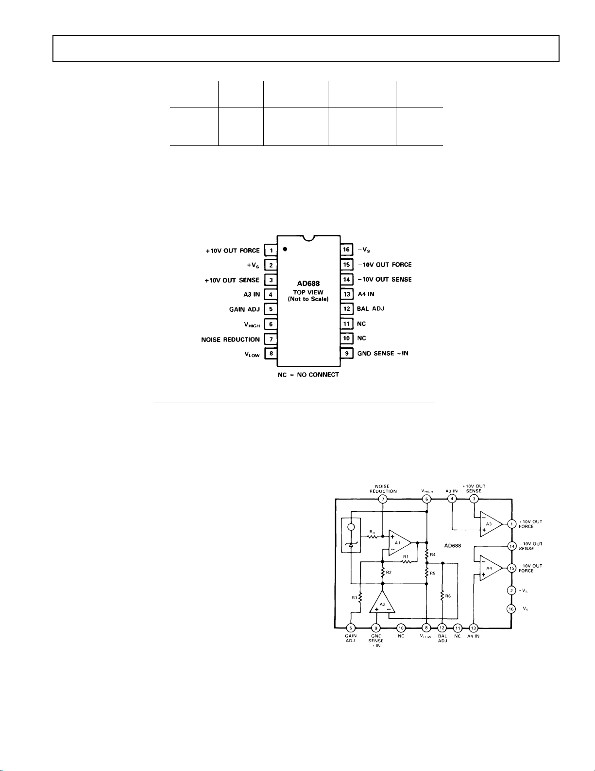
PIN CONFIGURATION
AD688
THEORY OF OPERATION
The AD688 consists of a buried Zener diode reference, amplifiers and associated thin-film resistors as shown in the block
diagram of Figure 1. The temperature compensation circuitry
provides the device with a temperature coefficient of 1.5 ppm/°C
or less.
Amplifier A1 performs several functions. A1 primarily acts to
amplify the Zener voltage to the required 20 volts. In addition,
A1 also provides for external adjustment of the 20 V output
through Pin 5, the GAIN ADJUST. Using the bias compensation resistor between the Zener output and the noninverting
input to A1, a capacitor can be added at the NOISE
REDUCTION pin (Pin 7) to form a low pass filter and reduce
the noise contribution of the Zener to the circuit. Two matched
12 kΩ nominal thin-film resistors (R4 and R5) divide the 20 V
output in half.
Ground sensing for the circuit is provided by Amplifier A2. The
noninverting input (Pin 9) senses the system ground and forces
the midpoint of resistors R4 and R5 to be a virtual ground. Pin
12 (BALANCE ADJUST) can be used for fine adjustment of
this midpoint transfer.
Amplifiers A3 and A4 are internally compensated and are used
to buffer the voltages at Pins 6 and 8 as well as to provide a full
Kelvin output. Thus, the AD688 has a full Kelvin capability by
providing the means to sense a system ground and provide
forced and sensed outputs referenced to that ground.
Figure 1. AD688 Functional Block Diagram
REV. A
–3–
Loading...