


 Loading...
Analog Devices AD678TD, AD678SD, AD678KN, AD678KD, AD678JN Datasheet
...a |
12-Bit 200 kSPS |
|
Complete Sampling ADC |
||
|
|
|
|
|
AD678* |
|
|
|
FEATURES
AC and DC Characterized and Specified (K, B and T Grades)
200k Conversions per Second
1 MHz Full Power Bandwidth
500 kHz Full Linear Bandwidth
72 dB S/N+D (K, B, T Grades)
Twos Complement Data Format (Bipolar Mode) Straight Binary Data Format (Unipolar Mode) 10 M Input Impedance
8-Bit or 16-Bit Bus Interface On-Board Reference and Clock
10 V Unipolar or Bipolar Input Range Commercial, Industrial and Military Temperature
Range Grades
MIL-STD-883 Compliant Versions Available
FUNCTIONAL BLOCK DIAGRAM
CS SC OE EOCEN SYNC 12/8 EOC
|
|
|
AD678 |
|
|
|
CONTROL LOGIC |
|
|
||
REFOUT |
VOLTAGE |
|
|
|
|
REF. |
|
12 |
DB11 |
||
REFIN |
|
|
DB2 |
||
|
|
OUTPUT |
|||
|
|
12 |
DB1 |
||
|
|
REGISTER |
|||
|
|
(R/L) |
|||
|
12-BIT D/A |
CONVERSION |
|||
|
DB0 |
||||
|
CONVERTER |
LOGIC |
|
||
|
|
|
|
(HBE) |
|
BIPOFF |
|
|
4 |
VCC |
|
|
SAMPLE/ |
GAIN |
4-BIT FLASH |
VEE |
|
AIN |
A/D |
VDD |
|||
HOLD |
STAGE |
||||
|
|
|
CONVERTER |
DGND |
|
AGND |
|
|
|
||
|
|
|
|
||
PRODUCT DESCRIPTION
The AD678 is a complete, multipurpose 12-bit monolithic analog-to-digital converter, consisting of a sample-hold amplifier (SHA), a microprocessor compatible bus interface, a voltage reference and clock generation circuitry.
The AD678 is specified for ac (or “dynamic”) parameters such as S/N+D ratio, THD and IMD which are important in signal processing applications. In addition, the AD678K, B and T grades are fully specified for dc parameters which are important in measurement applications.
The AD678 offers a choice of digital interface formats; the 12 data bits can be accessed by a 16-bit bus in a single read operation or by an 8-bit bus in two read operations (8+4), with right or left justification. Data format is straight binary for unipolar mode and twos complement binary for bipolar mode. The input has a full-scale range of 10 V with a full power bandwidth of
1 MHz and a full linear bandwidth of 500 kHz. High input impedance (10 MΩ) allows direct connection to unbuffered sources without signal degradation.
This product is fabricated on Analog Devices’ BiMOS process, combining low power CMOS logic with high precision, low noise bipolar circuits; laser-trimmed thin-film resistors provide high accuracy. The converter utilizes a recursive subranging algorithm which includes error correction and flash converter circuitry to achieve high speed and resolution.
The AD678 operates from +5 V and ±12 V supplies and dissipates 560 mW (typ). The AD678 is available in 28-lead plastic DIP, ceramic DIP, and 44-lead J-leaded ceramic surface mount packages.
Screening to MIL-STD-883C Class B is also available.
*Protected by U.S. Patent Nos. 4,804,960; 4,814,767; 4,833,345; 4,250,445; 4,808,908; RE30,586.
REV. C
Information furnished by Analog Devices is believed to be accurate and reliable. However, no responsibility is assumed by Analog Devices for its use, nor for any infringements of patents or other rights of third parties which may result from its use. No license is granted by implication or otherwise under any patent or patent rights of Analog Devices.
PRODUCT HIGHLIGHTS
1.COMPLETE INTEGRATION: The AD678 minimizes external component requirements by combining a high speed sample-hold amplifier (SHA), ADC, 5 V reference, clock and digital interface on a single chip. This provides a fully specified sampling A/D function unattainable with discrete designs.
2.SPECIFICATIONS: The AD678K, B and T grades provide fully specified and tested ac and dc parameters. The AD678J, A and S grades are specified and tested for ac parameters; dc accuracy specifications are shown as typicals. DC specifications (such as INL, gain and offset) are important in control and measurement applications. AC specifications (such as S/N+D ratio, THD and IMD) are of value in signal processing applications.
3.EASE OF USE: The pinout is designed for easy board layout, and the choice of single or two read cycle output provides compatibility with 16or 8-bit buses. Factory trimming eliminates the need for calibration modes or external trimming to achieve rated performance.
4.RELIABILITY: The AD678 utilizes Analog Devices’ monolithic BiMOS technology. This ensures long-term reliability compared to multichip and hybrid designs.
5.UPGRADE PATH: The AD678 provides the same pinout as the 14-bit, 128 kSPS AD679 ADC.
6.The AD678 is available in versions compliant with MIL- STD-883. Refer to the Analog Devices Military Products Databook or current AD678/883B data sheet for detailed specifications.
One Technology Way, P.O. Box 9106, Norwood, MA 02062-9106, U.S.A.
Tel: 781/329-4700 |
World Wide Web Site: http://www.analog.com |
Fax: 781/326-8703 |
© Analog Devices, Inc., 2000 |

AD678–SPECIFICATIONS
(TMIN to TMAX, VCC = +12 V 5%, VEE = –12 V 5%, VDD = +5 V 10%, fSAMPLE = 200 kSPS,
AC SPECIFICATIONS flN = 10.06 kHz unless otherwise noted)1
|
|
AD678J/A/S |
|
AD678K/B/T |
|
||
Parameter |
Min |
Typ |
Max |
Min |
Typ |
Max |
Units |
|
|
|
|
|
|
|
|
SIGNAL-TO-NOISE AND DISTORTION (S/N+D) RATIO2 |
|
|
|
|
|
|
|
–0.5 dB Input (Referred to –0 dB Input) |
70 |
71 |
|
71 |
73 |
|
dB |
–20 dB Input (Referred to –20 dB Input) |
|
51 |
|
|
53 |
|
dB |
–60 dB Input (Referred to –60 dB Input) |
|
11 |
|
|
13 |
|
dB |
|
|
|
|
|
|
|
|
TOTAL HARMONIC DISTORTION (THD)3 |
|
–88 |
–80 |
|
–88 |
–80 |
dB |
|
|
0.004 |
0.010 |
|
0.004 |
0.010 |
% |
|
|
|
|
|
|
|
|
PEAK SPURIOUS OR PEAK HARMONIC COMPONENT |
|
–87 |
–80 |
|
–87 |
–80 |
dB |
|
|
|
|
|
|
|
|
FULL POWER BANDWIDTH |
|
1 |
|
|
1 |
|
MHz |
|
|
|
|
|
|
|
|
FULL LINEAR BANDWIDTH |
500 |
|
|
500 |
|
|
kHz |
|
|
|
|
|
|
|
|
INTERMODULATION DISTORTION (IMD)4 |
|
|
|
|
|
|
|
2nd Order Products |
|
–85 |
–80 |
|
–85 |
–80 |
dB |
3rd Order Products |
|
–90 |
–80 |
|
–90 |
–80 |
dB |
|
|
|
|
|
|
|
|
NOTES
1fIN amplitude = –0.5 dB (9.44 V p-p) bipolar mode full scale unless otherwise indicated. All measurements referred to a –0 dB (9.997 V p-p) input signal unless otherwise indicated.
2See Figures 13 and 14 for higher frequencies and other input amplitudes. 3See Figure 12.
4fA = 9.08 kHz, fB = 9.58 kHz, with fSAMPLE = 200 kSPS. See Definition of Specifications section and Figure 16. Specifications subject to change without notice.
DIGITAL SPECIFICATIONS (All device types TMIN to TMAX, VCC = +12 V 5%, VEE = –12 V 5%, VDD = +5 V 10%)
Parameter |
Test Conditions |
Min |
Max |
Units |
|
|
|
|
|
|
|
LOGIC INPUTS |
|
|
|
|
|
VIH |
High Level Input Voltage |
|
2.0 |
VDD |
V |
VIL |
Low Level Input Voltage |
|
0 |
0.8 |
V |
IIH |
High Level Input Current |
VIN = VDD |
–10 |
+10 |
A |
IIL |
Low Level Input Current |
VIN = 0 V |
–10 |
+10 |
A |
CIN |
Input Capacitance |
|
|
10 |
pF |
LOGIC OUTPUTS |
|
|
|
|
|
VOH |
High Level Output Voltage |
IOH = 0.1 mA |
4.0 |
|
V |
VOL |
|
IOH = 0.5 mA |
2.4 |
|
V |
Low Level Output Voltage |
IOL = 1.6 mA |
|
0.4 |
V |
|
IOZ |
High Z Leakage Current |
VIN = 0 or VDD |
–10 |
+10 |
A |
COZ |
High Z Output Capacitance |
|
|
10 |
pF |
Specifications subject to change without notice.
–2– |
REV. C |
|
|
|
|
|
|
|
AD678 |
|
DC SPECIFICATIONS (TMIN to TMAX, VCC = +12 V 5%, VEE = –12 V 5%, VDD = +5 V 10% unless otherwise noted) |
|
|
||||||
|
|
|
|
|
|
|
|
|
|
|
AD678J/A/S |
|
|
AD678K/B/T |
|
|
|
Parameter |
Min |
Typ |
Max |
Min |
Typ |
Max |
Units |
|
|
|
|
|
|
|
|
|
|
TEMPERATURE RANGE |
|
|
|
|
|
|
°C |
|
J, K Grades |
0 |
|
+70 |
0 |
|
+70 |
||
A, B Grades |
–40 |
|
+85 |
–40 |
|
+85 |
°C |
|
S, T Grades |
–55 |
|
+125 |
–55 |
|
+125 |
°C |
|
ACCURACY |
|
|
|
|
|
|
|
|
Resolution |
12 |
±1 |
|
12 |
±0.7 |
±1 |
Bits |
|
Integral Nonlinearity (INL) |
|
|
|
LSB |
||||
Differential Nonlinearity (DNL) |
12 |
±4 |
|
12 |
±2 |
±3 |
Bits |
|
Unipolar Zero Error (@ +25°C)1 |
|
|
|
LSB |
||||
Bipolar Zero Error (@ +25°C)1 |
|
±4 |
|
|
±3 |
±5 |
LSB |
|
Gain Error (@ +25°C)1, 2 |
|
±4 |
|
|
±3 |
±6 |
LSB |
|
Temperature Drift |
|
|
|
|
|
|
|
|
Unipolar/Bipolar Zero |
|
±2 |
|
|
±2 |
±4 |
|
|
J, K Grades |
|
|
|
LSB |
||||
A, B Grades |
|
±4 |
|
|
±3 |
±4 |
LSB |
|
S, T Grades |
|
±5 |
|
|
±4 |
±5 |
LSB |
|
Gain3 |
|
±4 |
|
|
±4 |
±6 |
|
|
J, K Grades |
|
|
|
LSB |
||||
A, B Grades |
|
±7 |
|
|
±5 |
±9 |
LSB |
|
S, T Grades |
|
±10 |
|
|
±8 |
±10 |
LSB |
|
Gain4 |
|
±2 |
|
|
±2 |
±4 |
|
|
J, K Grades |
|
|
|
LSB |
||||
A, B Grades |
|
±4 |
|
|
±3 |
±4 |
LSB |
|
S, T Grades |
|
±6 |
|
|
±5 |
±6 |
LSB |
|
ANALOG INPUT |
|
|
|
|
|
|
|
|
Input Ranges |
|
|
|
|
|
|
|
|
Unipolar Range |
0 |
|
+10 |
0 |
|
+10 |
V |
|
Bipolar Range |
–5 |
|
+5 |
–5 |
|
+5 |
V |
|
Input Resistance |
|
10 |
|
|
10 |
|
MΩ |
|
Input Capacitance |
|
10 |
|
|
10 |
|
pF |
|
Input Settling Time |
|
|
1 |
|
|
1 |
µs |
|
Aperture Delay |
|
10 |
|
|
10 |
|
ns |
|
Aperture Jitter |
|
150 |
|
|
150 |
|
ps |
|
|
|
|
|
|
|
|
|
|
INTERNAL VOLTAGE REFERENCE |
|
|
|
|
|
|
|
|
Output Voltage5 |
4.98 |
|
5.02 |
4.98 |
|
5.02 |
V |
|
External Load |
|
|
|
|
|
|
|
|
Unipolar Mode |
|
|
+1.5 |
|
|
+1.5 |
mA |
|
Bipolar Mode |
|
|
+0.5 |
|
|
+0.5 |
mA |
|
|
|
|
|
|
|
|
|
|
POWER SUPPLIES |
|
|
|
|
|
|
|
|
Power Supply Rejection |
|
|
|
|
|
|
|
|
VCC = +12 V ± 5% |
|
±2 |
|
|
|
±2 |
LSB |
|
VEE = –12 V ± 5% |
|
±2 |
|
|
|
±2 |
LSB |
|
VDD = +5 V ± 10% |
|
±2 |
|
|
|
±2 |
LSB |
|
Operating Current |
|
|
|
|
|
|
|
|
ICC |
|
18 |
20 |
|
18 |
20 |
mA |
|
IEE |
|
25 |
34 |
|
25 |
34 |
mA |
|
IDD |
|
8 |
12 |
|
8 |
12 |
mA |
|
Power Consumption |
|
560 |
745 |
|
560 |
745 |
mW |
|
|
|
|
|
|
|
|
|
|
NOTES 1Adjustable to zero.
2Includes internal voltage reference error.
3Includes internal voltage reference drift.
4Excludes internal voltage reference drift.
5With maximum external load applied.
Specifications subject to change without notice.
REV. C |
–3– |
AD678
TIMING SPECIFICATIONS
(All grades, TMIN to TMAX, VCC = +12 V 5%, VEE = –12 V 5%, VDD = +5 V 10% unless otherwise noted)
Parameter |
Symbol |
Min |
Max |
Units |
|
|
|
|
|
SC Delay |
tSC |
50 |
|
ns |
Conversion Time |
tC |
3.0 |
4.4 |
s |
Conversion Ratel |
tCR |
|
5 |
s |
Convert Pulsewidth |
tCP |
97 |
|
ns |
Aperture Delay |
tAD |
5 |
20 |
ns |
Status Delay |
tSD |
0 |
400 |
ns |
Access Time2, 3 |
tBA |
10 |
100 |
ns |
Float Delay5 |
|
10 |
574 |
ns |
tFD |
10 |
80 |
ns |
|
Output Delay |
tOD |
|
0 |
ns |
Format Setup |
tFS |
47 |
|
ns |
OE Delay |
tOE |
0 |
|
ns |
Read Pulsewidth |
tRP |
97 |
|
ns |
Conversion Delay |
tCD |
150 |
|
ns |
EOCEN Delay |
tEO |
0 |
|
ns |
NOTES
1Includes acquisition time.
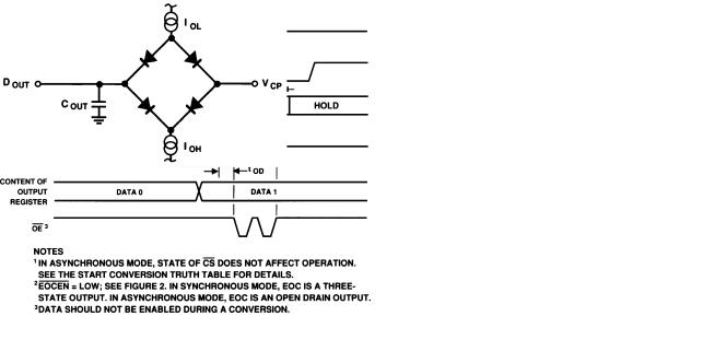
2Measured from the falling edge of OE/EOCEN (0.8 V) to the time at which the data lines/EOC cross 2.0 V or 0.8 V. See Figure 3. 3COUT = 100 pF.
4COUT = 50 pF.
5Measured from the rising edge of OE/EOCEN (2.0 V) to the time at which the output voltage changes by 0.5 V. See Figure 3; COUT = 10 pF. Specifications subject to change without notice.
Figure 2. EOC Timing
Figure 1. Conversion Timing
Figure 3. Load Circuit for Bus Timing Specifications
–4– |
REV. C |

AD678
ABSOLUTE MAXIMUM RATINGS*
|
With |
|
|
|
|
Respect |
|
|
|
Specification |
To |
Min |
Max |
Units |
|
|
|
|
|
VCC |
AGND |
–0.3 |
+18 |
V |
VEE |
AGND |
–18 |
+0.3 |
V |
VCC |
VEE |
–0.3 |
+26.4 |
V |
VDD |
DGND |
0 |
+7 |
V |
AGND |
DGND |
–1 |
+1 |
V |
AIN, REFIN |
AGND |
VEE |
VCC |
V |
Digital Inputs |
DGND |
–0.5 |
+7 |
V |
Digital Outputs |
DGND |
–0.5 |
VDD + 0.3 |
V |
Max Junction |
|
|
|
°C |
Temperature |
|
|
175 |
|
Operating Temperature |
|
|
|
°C |
J and K Grades |
|
0 |
+70 |
|
A and B Grades |
|
–40 |
+85 |
°C |
S and T Grades |
|
–55 |
+125 |
°C |
Storage Temperature |
|
–65 |
+150 |
°C |
Lead Temperature |
|
|
|
°C |
(10 sec max) |
|
|
+300 |
|
|
|
|
|
|
CS SC OE EOCEN SYNC 12/8 EOC
|
|
|
AD678 |
|
|
|
CONTROL LOGIC |
|
|
||
REFOUT |
VOLTAGE |
|
|
|
|
REF. |
|
12 |
DB11 |
||
REFIN |
|
|
DB2 |
||
|
|
OUTPUT |
|||
|
|
12 |
DB1 |
||
|
|
REGISTER |
|||
|
|
(R/L) |
|||
|
12-BIT D/A |
CONVERSION |
|||
|
DB0 |
||||
|
CONVERTER |
LOGIC |
|
||
|
|
|
|
(HBE) |
|
BIPOFF |
|
|
4 |
VCC |
|
|
SAMPLE/ |
GAIN |
4-BIT FLASH |
VEE |
|
AIN |
A/D |
VDD |
|||
HOLD |
STAGE |
||||
|
|
|
CONVERTER |
DGND |
|
AGND |
|
|
|
||
|
|
|
|
||
Functional Block Diagram
*Stresses above those listed under Absolute Maximum Ratings may cause permanent damage to the device. This is a stress rating only; functional operation of the device at these or any other conditions above those indicated in the operational sections of this specification is not implied. Exposure to absolute maximum rating conditions for extended periods may affect device reliability.
ESD SENSITIVITY
The AD678 features input protection circuitry consisting of large “distributed” diodes and polysilicon series resistors to dissipate both high energy discharges (Human Body Model) and fast, low energy pulses (Charged Device Model). Per Method 3015.2 of MIL-STD-883C, the AD678 has been classified as a Category 1 device.
Proper ESD precautions are strongly recommended to avoid functional damage or performance degradation. Charges as high as 4000 volts readily accumulate on the human body and test equipment and discharge without detection. Unused devices must be stored in conductive foam or shunts, and the foam should be discharged to the destination socket before devices are removed. For further information on ESD precautions, refer to Analog Devices’ ESD Prevention Manual.
WARNING!
ESD SENSITIVE DEVICE
ORDERING GUIDE
Model1 |
Package |
Temperature Range |
Tested and Specified |
Package Option2 |
AD678JN |
28-Lead Plastic DIP |
0°C to +70°C |
AC |
N-28 |
AD678KN |
28-Lead Plastic DIP |
0°C to +70°C |
AC + DC |
N-28 |
AD678JD |
28-Lead Ceramic DIP |
0°C to +70°C |
AC |
D-28 |
AD678KD |
28-Lead Ceramic DIP |
0°C to +70°C |
AC + DC |
D-28 |
AD678AD |
28-Lead Ceramic DIP |
–40°C to +85°C |
AC |
D-28 |
AD678BD |
28-Lead Ceramic DIP |
–40°C to +85°C |
AC + DC |
D-28 |
AD678AJ |
44-Lead Ceramic JLCC |
–40°C to +85°C |
AC |
J-44 |
AD678BJ |
44-Lead Ceramic JLCC |
–40°C to +85°C |
AC + DC |
J-44 |
AD678SD |
28-Lead Ceramic DIP |
–55°C to +125°C |
AC |
D-28 |
AD678TD |
28-Lead Ceramic DIP |
–55°C to +125°C |
AC + DC |
D-28 |
NOTES
1For details on grade and package offerings screened in accordance with MIL-STD-883, refer to Analog Devices Military Products Databook or /883 data sheet. 2N = Plastic DIP; D = Ceramic DIP; J = J-Leaded Ceramic Chip Carrier.
REV. C |
–5– |
Loading...