


AD674BBR
Table of contents
 Loading...
Analog Devices AD674BBR, AD674BBD, AD674BAR, AD674BTD, AD674BKN Datasheet
...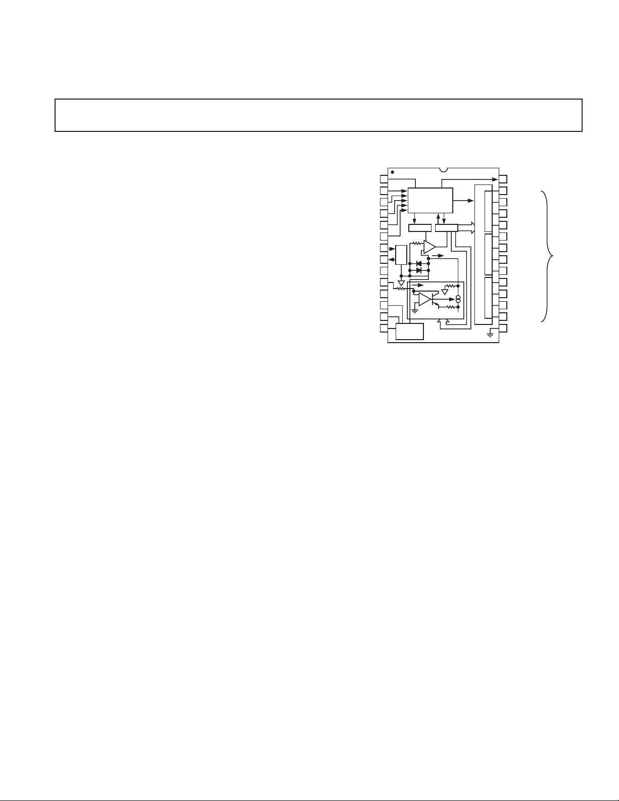
FUNCTIONAL BLOCK DIAGRAM
28
27
26
25
24
23
22
21
20
19
18
17
16
15
1
2
3
4
5
6
7
8
9
10
11
12
13
14
AD674B/AD774B
5V SUPPLY
V
LOGIC
DATA MODE SELECT
12/8
CHIP SELECT
CS
BYTE ADDRESS/
SHORT CYCLE A
0
READ/CONVERT R/C
CHIP ENABLE
CE
12V/15V SUPPLY
V
CC
10V REFERENCE
REF OUT
ANALOG COMMON
AC
REFERENCE INPUT
REF IN
–12V/–15V SUPPLY
V
EE
BIPOLAR OFFSET
BIPOFF
10V SPAN INPUT
10V
IN
20V SPAN INPUT
20V
IN
STATUS
STS
DB11 (MSB)
DB10
DB9
DB8
DB7
DB6
DB5
DB4
DB3
DB2
DB1
DB0 (LSB)
DIGITAL
COMMON DC
CONTROL
VO LTAG E
DIVIDER
N
Y
B
B
L
E
A
MSB
3
S
T
A
T
E
O
U
T
P
U
T
B
U
F
F
E
R
S
LSB
N
Y
B
B
L
E
B
N
Y
B
B
L
E
C
CLOCK SAR
12
10V
REF
–
+
COMP
I DAC
–
+
199.95
k
DAC
N
V
EE
I REF
DIGITAL
DATA
OUTPUTS
REV. C
Information furnished by Analog Devices is believed to be accurate and
reliable. However, no responsibility is assumed by Analog Devices for its
use, nor for any infringements of patents or other rights of third parties that
may result from its use. No license is granted by implication or otherwise
under any patent or patent rights of Analog Devices.
a
Complete 12-Bit
A/D Converters
AD674B
*
/AD774B
*
FEATURES
Complete Monolithic 12-Bit A/D Converters with
Reference, Clock, and Three-State Output Buffers
Industry Standard Pinout
High Speed Upgrades for AD574A
8- and 16-Bit Microprocessor Interface
8 s (Max) Conversion Time (AD774B)
15 s (Max) Conversion Time (AD674B)
5 V, 10 V, 0 V–10 V, 0 V–20 V Input Ranges
Commercial, Industrial, and Military Temperature
Range Grades
MIL-STD-883-Compliant Versions Available
PRODUCT DESCRIPTION
The AD674B and AD774B are complete 12-bit successive-
approximation analog-to-digital converters with three-state
output buffer circuitry for direct interface to 8- and 16-bit
microprocessor busses. A high-precision voltage reference and
clock are included on chip, and the circuit requires only power
supplies and control signals for operation.
The AD674B and AD774B are pin-compatible with the indus-
try standard AD574A, but offer faster conversion time and bus-
access speed than the AD574A and lower power consumption.
The AD674B converts in 15 µs (maximum) and the AD774B
converts in 8 µs (maximum).
The monolithic design is implemented using Analog Devices’
BiMOS II process allowing high-performance bipolar analog
circuitry to be combined on the same die with digital CMOS logic.
Offset, linearity, and scaling errors are minimized by active
laser trimming of thin-film resistors.
Five different grades are available. The J and K grades are
specified for operation over the 0°C to 70°C temperature range.
The A and B grades are specified from –40°C to +85°C, the T grade
is specified from –55°C to +125°C. The J and K grades are
available in a 28-lead plastic DIP or 28-lead SOIC. All other grades
are available in a 28-lead hermetically sealed ceramic DIP.
PRODUCT HIGHLIGHTS
1. Industry Standard Pinout: The AD674B and AD774B use
the pinout established by the industry standard AD574A.
2. Analog Operation: The precision, laser-trimmed scaling and
bipolar offset resistors provide four calibrated ranges: 0 V to
10 V and 0 V to 20 V unipolar; –5 V to +5 V and –10 V to
+10 V bipolar. The AD674B and AD774B operate on +5 V
and ± 12 V or ± 15 V power supplies.
3. Flexible Digital Interface: On-chip multiple-mode three-state
output buffers and interface logic allow direct connection to
most microprocessors. The 12 bits of output data can be
read either as one 12-bit word or as two 8-bit bytes (one with
8 data bits, the other with 4 data bits and 4 trailing zeros).
4. The internal reference is trimmed to 10.00 V with 1% maxi-
mum error and 10 ppm/°C typical temperature coefficient.
The reference is available externally and can drive up to
2.0 mA beyond the requirements of the converter and bipo-
lar offset resistors.
5. The AD674B and AD774B are available in versions compli-
ant with MIL-STD-883. Refer to the Analog Devices Mili-
tary Products Databook or current AD674B/AD774B/883B
data sheet for detailed specifications.
One Technology Way, P.O. Box 9106, Norwood, MA 02062-9106, U.S.A.
Tel: 781/329-4700 www.analog.com
Fax: 781/326-8703 © Analog Devices, Inc., 2002
*Protected by U.S. Patent Nos. 4,250,445; 4,808,908; RE30586.
J Grade K Grade A Grade B Grade T Grade
Model (AD674B or AD774B) Min Typ Max Min Typ Max Min Typ Max Min Typ Max Min Typ Max Unit
RESOLUTION 12 12 12 12 12 Bits
LINEARITY ERROR @ 25°C 1 1/2 1 1/2 1/2 LSB
T
MIN
to T
MAX
1 1/2 1 1/2 1 LSB
DIFFERENTIAL LINEARITY ERROR
(Minimum Resolution for Which No
Missing Codes are Guaranteed) 12 12 12 12 12 Bits
UNIPOLAR OFFSET
1
@ 25°C 2 2 2 2 2 LSB
BIPOLAR OFFSET
1
@ 25°C 6 3 6 3 3 LSB
FULL-SCALE CALIBRATION ERROR
1, 2
@ 25°C (with Fixed 50 Ω Resistor
from REF OUT to REF IN) 0.1 0.25 0.1 0.125 0.1 0.25 0.1 0.125 0.1 0.125 % of FS
TEMPERATURE RANGE 0 70 0 70 –40 +85 –40 +85 –55 +125 °C
TEMPERATURE DRIFT
3
(Using Internal Reference)
Unipolar 2 1 2 1 1 LSB
Bipolar Offset 2 1 2 1 2 LSB
Full-Scale Calibration 6 2 8 5 7 LSB
POWER SUPPLY REJECTION
Max Change in Full-Scale Calibration
V
CC
= +15 V ± 1.5 V or +12 V ± 0.6 V 2 1 2 1 1 LSB
V
LOGIC
= +5 V ± 0.5 V 1/2 1/2 1/2 1/2 1/2 LSB
V
EE
= –15 V ± 1.5 V or –12 V ± 0.6 V 2 1 2 1 1 LSB
ANALOG INPUT
Input Ranges
Bipolar –5 +5 –5 +5 –5 +5 –5 +5 –5 +5 V
–10 +10 –10 +10 –10 +10 –10 +10 –10 +10 V
Unipolar 0 10 0 10 0 10 0 10 0 10 V
0 20 0 20 0 20 0 20 0 20 V
Input Impedance
10 V Span 3 5 735 735 735 735 7 kΩ
20 V Span 6 10 14 6 10 14 6 10 14 6 10 14 6 10 14 kΩ
POWER SUPPLIES
Operating Range
V
LOGIC
4.5 5.5 4.5 5.5 4.5 5.5 4.5 5.5 4.5 5.5 V
V
CC
11.4 16.5 11.4 16.5 11.4 16.5 11.4 16.5 11.4 16.5 V
V
EE
–16.5 –11.4 –16.5 –11.4 –16.5 –11.4 –16.5 –11.4 –16.5 –11.4 V
Operating Current
I
LOGIC
3.5 7 3.5 7 3.5 7 3.5 7 3.5 7 mA
I
CC
3.5 7 3.5 7 3.5 7 3.5 7 3.5 7 mA
I
EE
10 14 10 14 10 14 10 14 10 14 mA
POWER CONSUMPTION 220 375 220 375 220 375 220 375 220 375 mW
4
175 175 175 175 175 mW
5
INTERNAL REFERENCE VOLTAGE 9.9 10.0 10.1 9.9 10.0 10.1 9.9 10.0 10.1 9.9 10.0 10.1 9.9 10.0 10.1 V
Output Current
(Available for External Loads) 2.0 2.0 2.0 2.0 2.0 mA
(External Load Should Not
Change During the Conversion)
NOTES
1
Adjustable to zero.
2
Includes internal voltage reference error.
3
Maximum change from 25°C value to the value at T
MIN
or T
MAX
.
4
Tested with REF OUT tied to REF IN through 50 Ω resistor, V
CC
= +16.5 V, V
EE
= –16.5 V, V
LOGIC
= +5.5 V, and outputs in high-Z mode.
5
Tested with REF OUT tied to REF IN through 50 Ω resistor, V
CC
= +12 V, V
EE
= –12 V, V
LOGIC
= +5 V, and outputs in high-Z mode.
Specifications subject to change without notice.
Specifications shown in boldface are tested on all devices at final electrical test at T
MIN
, 25°C, and T
MAX
. Results from those tests are used to calculate outgoing quality levels. All min and
max specifications are guaranteed, although only those shown in boldface are tested.
AD674B/AD774B–SPECIFICATIONS
(T
MIN
to T
MAX
with V
CC
= +15 V 10% or +12 V 5%,
V
LOGIC
= +5 V 10%, V
EE
= –15 V 10% or –12 V 5%, unless otherwise noted.)
REV. C
–2–
REV. C
–3–
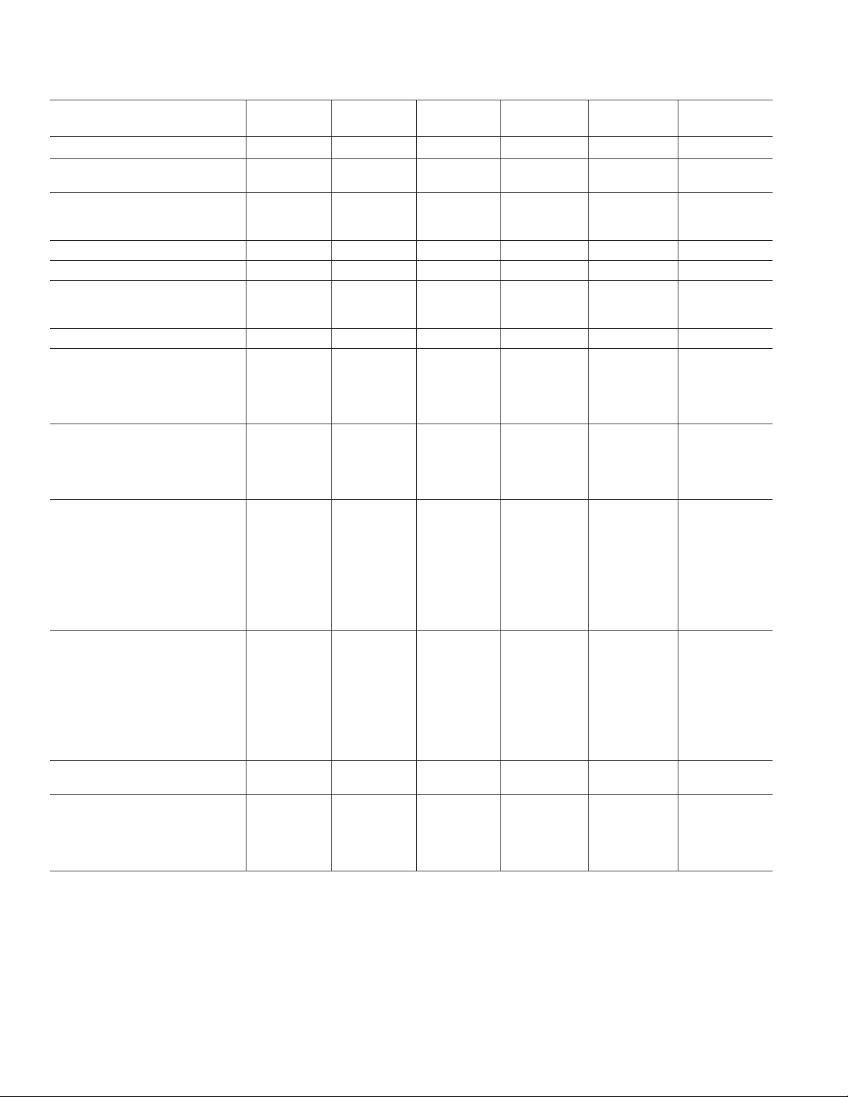
CONVERTER START TIMING (Figure 1)
J, K, A, B Grades T Grade
Parameter Symbol Min Typ Max Min Typ Max Unit
Conversion Time
8-Bit Cycle (AD674B) t
C
6810 6810 µs
12-Bit Cycle (AD674B) t
C
91215 91215 µs
8-Bit Cycle (AD774B) t
C
456 456 µs
12-Bit Cycle (AD774B) t
C
6 7.3 8 6 7.3 8 µs
STS Delay from CE t
DSC
200 225 ns
CE Pulsewidth t
HEC
50 50 ns
CS to CE Setup t
SSC
50 50 ns
CS Low During CE High t
HSC
50 50 ns
R/C to CE Setup t
SRC
50 50 ns
R/C LOW During CE High t
HRC
50 50 ns
A
0
to CE Setup t
SAC
00ns
A
0
Valid During CE High t
HAC
50 50 ns
READ TIMING—FULL CONTROL MODE (Figure 2)
J, K, A, B Grades T Grade
Parameter Symbol Min Typ Max Min Typ Max Unit
Access Time
C
L
= 100 pF t
DD
1
75 150 75 150 ns
Data Valid After CE Low t
HD
25
2
25
2
ns
20
3
15
4
ns
Output Float Delay t
HL
5
150 150 ns
CS to CE Setup t
SSR
50 50 ns
R/C to CE Setup t
SRR
00ns
A
0
to CE Setup t
SAR
50 50 ns
CS Valid After CE Low t
HSR
00ns
R/C High After CE Low t
HRR
00ns
A
0
Valid After CE Low t
HAR
50 50 ns
NOTES
1
t
DD
is measured with the load circuit of Figure 3a and is defined as the time required
for an output to cross 0.4 V or 2.4 V.
2
0°C to T
MAX
.
3
At –40°C.
4
At –55°C.
5
t
HL
is defined as the time required for the data lines to change 0.5 V when loaded with
the circuit of Figure 3b.
Specifications shown in boldface are tested on all devices at final electrical test with
worst case supply voltages at T
MIN
, 25°C, and T
MAX
. Results from those tests are used
to calculate outgoing quality levels. All min and max specifications are guaranteed,
although only those shown in boldface are tested.
Specifications subject to change without notice.
Parameter Test Conditions Min Max Unit
LOGIC INPUTS
V
IH
High Level Input Voltage 2.0 V
LOGIC
+ 0.5 V
V
IL
Low Level Input Voltage –0.5 +0.8 V
I
IH
High Level Input Current V
IN
= V
LOGIC
–10 +10 µA
I
IL
Low Level Input Current V
IN
= 0 V –10 +10 µA
C
IN
Input Capacitance 10 pF
LOGIC OUTPUTS
V
OH
High Level Output Voltage I
OH
= 0.5 mA 2.4 V
V
OL
Low Level Output Voltage I
OL
= 1.6 mA 0.4 V
I
OZ
High-Z Leakage Current V
IN
= 0 to V
LOGIC
–10 +10 µA
C
OZ
High-Z Output Capacitance 10 pF
DIGITAL SPECIFICATIONS
(For all grades T
MIN
to T
MAX
with V
CC
= +15 V 10% or +12 V 5%, V
LOGIC
= +5 V 10%,
V
EE
= –15 V 10% or –12 V 5%, unless otherwise noted.)
SWITCHING SPECIFICATIONS
(For all grades T
MIN
to T
MAX
with V
CC
= +15 V 10% or +12 V 5%,
V
LOGIC
= +5 V 10%, V
EE
= –15 V 10% or –12 V 5%, unless otherwise noted.)
t
HEC
t
HSC
t
SSC
t
HRC
t
SRC
t
SAC
t
HAC
t
C
t
DSC
CE
CS
R/C
A
0
STS
DB11 – DB0
HIGH
IMPEDANCE
Figure 1. Convert Start Timing
t
SSR
CE
CS
R/C
A
0
STS
DB11 – DB0
t
HSR
t
HRR
t
HAR
t
HD
t
SAR
t
SRR
HIGH
IMPEDANCE
DATA
VA LI D
HIGH
IMPEDANCE
t
HL
t
DD
Figure 2. Read Cycle Timing
DB
N
3k
100pF
DB
N
3k
100pF
5V
HIGH-Z TO LOGIC 0HIGH-Z TO LOGIC 1
High-Z to Logic 1 High-Z to Logic 0
Figure 3a. Load Circuit for Access Time Test
DB
N
3k
100pF
LOGIC 1 TO HIGH-Z
DB
N
3k
100pF
5V
LOGIC 0 TO HIGH-Z
Logic 1 to High-Z Logic 0 to High-Z
Figure 3b. Load Circuit for Output Float Delay Test
AD674B/AD774B
REV. C–4–
AD674B/AD774B
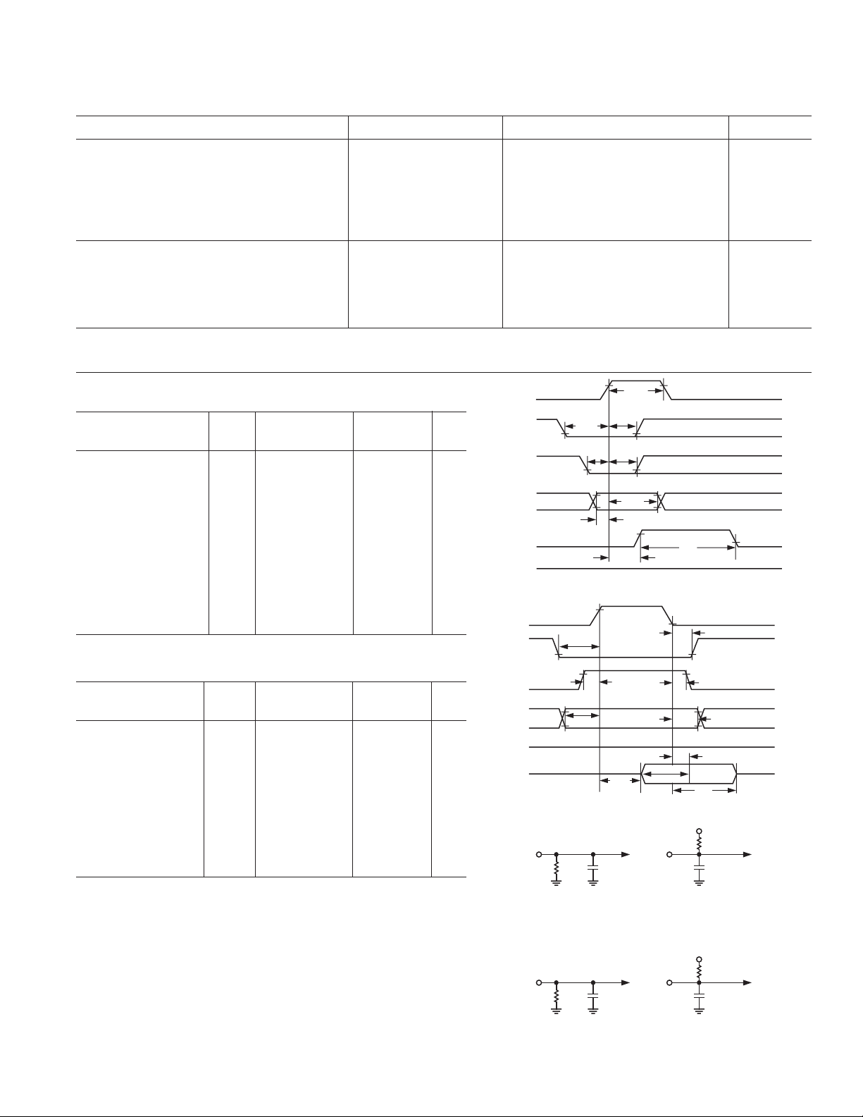
TIMING—STAND ALONE MODE (Figures 4a and 4b)
J, K, A, B Grades T Grade
Parameter Symbol Min Typ Max Min Typ Max Unit
Data Access Time t
DDR
150 150 ns
Low R/C Pulsewidth t
HRL
50 50 ns
STS Delay from R/C t
DS
200 225 ns
Data Valid After R/C Low t
HDR
25 25 ns
STS Delay After Data Valid t
HS
30 200 600 30 200 600 ns
High R/C Pulsewidth t
HRH
150 150 ns
Specifications subject to change without notice.
ABSOLUTE MAXIMUM RATINGS*
V
CC
to Digital Common . . . . . . . . . . . . . . . . . . . 0 to +16.5 V
V
EE
to Digital Common . . . . . . . . . . . . . . . . . . . . 0 to –16.5 V
V
LOGIC
to Digital Common . . . . . . . . . . . . . . . . . . . 0 to +7 V
Analog Common to Digital Common . . . . . . . . . . . . . . . ± 1 V
Digital Inputs to Digital Common . . . –0.5 V to V
LOGIC
+0.5 V
Analog Inputs to Analog Common . . . . . . . . . . . . V
EE
to V
CC
20 V
IN
to Analog Common . . . . . . . . . . . . . . . . . . . . . . ±24 V
REF OUT . . . . . . . . . . . . . . . . . . Indefinite Short to Common
. . . . . . . . . . . . . . . . . . . . . . . . . . . . . Momentary Short to V
CC
Junction Temperature . . . . . . . . . . . . . . . . . . . . . . . . . . 175°C
Power Dissipation . . . . . . . . . . . . . . . . . . . . . . . . . . . 825 mW
Lead Temperature, Soldering (10 sec) . . . . . . . . . . . . . 300°C
Storage Temperature . . . . . . . . . . . . . . . . . . –65°C to +150°C
*Stresses above those listed under Absolute Maximum Ratings may cause perma-
nent damage to the device. This is a stress rating only and functional operation of
the device at these or any other conditions above those indicated in the operational
section of this specification is not implied. Exposure to absolute maximum rating
conditions for extended periods may affect device reliability.
R/C
STS
DB11–DB0
DATA
VA LI D
DATA VAL ID
t
HRL
t
DS
HIGH–Z
t
HS
t
HDR
t
C
Flgure 4a. Standalone Mode Timing Low Pulse R/
C
R/C
STS
DB11–DB0
HIGH–Z HIGH–Z
DATA
VA LI D
t
HRH
t
DS
t
DDR
t
HDR
t
C
t
HL
Figure 4b. Standalone Mode Timing High Pulse for R/
C
WARNING!
ESD SENSITIVE DEVICE
CAUTION
ESD (electrostatic discharge) sensitive device. Electrostatic charges as high as 4000 V readily
accumulate on the human body and test equipment and can discharge without detection. Although
the AD674B/AD774B features proprietary ESD protection circuitry, permanent damage may occur
on devices subjected to high energy electrostatic discharges. Therefore, proper ESD precautions are
recommended to avoid performance degradation or loss of functionality.
ORDERING GUIDE
Conversion INL Package Package
Model
l
Temperature Time (max) (T
MIN
to T
MAX
) Description Option
2
AD674BJN 0°C to 70°C 15 µs ± 1 LSB Plastic DIP N-28
AD674BKN 0°C to 70°C 15 µs ± 1/2 LSB Plastic DIP N-28
AD674BAR –40°C to +85°C 15 µs ± 1 LSB Plastic SOIC R-28
AD674BBR –40°C to +85°C 15 µs ± 1/2 LSB Plastic SOIC R-28
AD674BAD –40°C to +85°C 15 µs ± 1 LSB Ceramic DIP D-28
AD674BBD –40°C to +85°C 15 µs ± 1/2 LSB Ceramic DIP D-28
AD674BTD –55°C to +125°C 15 µs ±1 LSB Ceramic DIP D-28
AD774BJN 0°C to 70°C8 µs ±1 LSB Plastic DIP N-28
AD774BKN 0°C to 70°C8 µs ± 1/2 LSB Plastic DIP N-28
AD774BAR –40°C to +85°C8 µs ±1 LSB Plastic SOIC R-28
AD774BBR –40°C to +85°C8 µs ± 1/2 LSB Plastic SOIC R-28
AD774BAD –40°C to +85°C8 µs ± 1 LSB Ceramic DIP D-28
AD774BBD –40°C to +85°C8 µs ± 1/2 LSB Ceramic DIP D-28
AD774BTD –55°C to +125°C8 µs ± 1 LSB Ceramic DIP D-28
NOTES
1
For details on grade and package offerings screened in accordance with MIL-STD-883, refer to the Analog Devices Military
Products Databook or the current AD674B/ AD774B/883B data sheet.
2
N = Plastic DIP; D = Hermetic DIP; R = Plastic SOIC.
Loading...