


AD670AD
Table of contents
 Loading...
Analog Devices AD670AD, AD670SD, AD670KN, AD670JP, AD670JN Datasheet
...
FUNCTIONAL BLOCK DIAGRAM
REV. A
Information furnished by Analog Devices is believed to be accurate and
reliable. However, no responsibility is assumed by Analog Devices for its
use, nor for any infringements of patents or other rights of third parties
which may result from its use. No license is granted by implication or
otherwise under any patent or patent rights of Analog Devices.
a
Low Cost Signal
Conditioning 8-Bit ADC
AD670
FEATURES
Complete 8-Bit Signal Conditioning A/D Converter
Including Instrumentation Amp and Reference
Microprocessor Bus Interface
10 ms Conversion Speed
Flexible Input Stage: Instrumentation Amp Front End
Provides Differential Inputs and High Common-Mode
Rejection
No User Trims Required
No Missing Codes Over Temperature
Single +5 V Supply Operation
Convenient Input Ranges
20-Pin DIP or Surface-Mount Package
Low Cost Monolithic Construction
MIL-STD-883B Compliant Versions Available
GENERAL DESCRIPTION
The AD670 is a complete 8-bit signal conditioning analog-
to-digital converter. It consists of an instrumentation amplifier
front end along with a DAC, comparator, successive approxima-
tion register (SAR), precision voltage reference, and a three-
state output buffer on a single monolithic chip. No external
components or user trims are required to interface, with full
accuracy, an analog system to an 8-bit data bus. The AD670
will operate on the +5 V system supply. The input stage pro-
vides differential inputs with excellent common-mode rejection
and allows direct interface to a variety of transducers.
The device is configured with input scaling resistors to permit
two input ranges: 0 mV to 255 mV (1 mV/LSB) and 0 to 2.55 V
(10 mV/LSB). The AD670 can be configured for both unipolar
and bipolar inputs over these ranges. The differential inputs and
common-mode rejection of this front end are useful in applica-
tions such as conversion of transducer signals superimposed on
common-mode voltages.
The AD670 incorporates advanced circuit design and proven
processing technology. The successive approximation function
is implemented with I
2
L (integrated injection logic). Thin-film
SiCr resistors provide the stability required to prevent missing
codes over the entire operating temperature range while laser
wafer trimming of the resistor ladder permits calibration of the
device to within ±1 LSB. Thus, no user trims for gain or offset
are required. Conversion time of the device is 10 µs.
The AD670 is available in four package types and five grades.
The J and K grades are specified over 0°C to +70°C and come
in 20-pin plastic DIP packages or 20-terminal PLCC packages.
The A and B grades (–40°C to +85°C) and the S grade (–55°C
to +125°C) come in 20-pin ceramic DIP packages.
One Technology Way, P.O. Box 9106, Norwood, MA 02062-9106, U.S.A.
Tel: 617/329-4700 Fax: 617/326-8703
The S grade is also available with optional processing to
MIL-STD-883 in 20-pin ceramic DIP or 20-terminal LCC
packages. The Analog Devices Military Products Databook
should be consulted for detailed specifications.
PRODUCT HIGHLIGHTS
1. The AD670 is a complete 8-bit A/D including three-state
outputs and microprocessor control for direct connection to
8-bit data buses. No external components are required to
perform a conversion.
2. The flexible input stage features a differential instrumenta-
tion amp input with excellent common-mode rejection. This
allows direct interface to a variety of transducers without
preamplification.
3. No user trims are required for 8-bit accurate performance.
4. Operation from a single +5 V supply allows the AD670 to
run off of the microprocessor’s supply.
5. Four convenient input ranges (two unipolar and two bipolar)
are available through internal scaling resistors: 0 mV to
255 mV (1 mV/LSB) and 0 V to 2.55 V (10 mV/LSB).
6. Software control of the output mode is provided. The user
can easily select unipolar or bipolar inputs and binary or 2s
complement output codes.

Model AD670J AD670K
Min Typ Max Min Typ Max Units
OPERATING TEMPERATURE RANGE 0 +70 0 +70 °C
RESOLUTION 8 8 Bit
CONVERSION TIME 10 10 µs
RELATIVE ACCURACY 61/2 61/4 LSB
T
MIN
to T
MAX
6l/2 61/2 LSB
DIFFERENTIAL LINEARITY ERROR
1
T
MIN
to T
MAX
GUARANTEED NO MISSING CODES ALL GRADES
GAIN ACCURACY
@ +25°C 61.5 60.75 LSB
T
MIN
to T
MAX
62.0 61.0 LSB
UNIPOLAR ZERO ERROR
@ +25°C 61.5 60.75 LSB
T
MIN
to T
MAX
62.0 61.0 LSB
BIPOLAR ZERO ERROR
@ +25°C 61.5 60.75 LSB
T
MIN
to T
MAX
62.0 61.0 LSB
ANALOG INPUT RANGES
DIFFERENTIAL (–V
IN
to +V
IN
)
Low Range 0 to +255 0 to +255 mV
–128 to +127 –128 to +127 mV
High Range 0 to +2.55 0 to +2.55 V
–1.28 to +1.27 –1.28 to +1.27 V
ABSOLUTE (Inputs to Power GND)
Low Range T
MIN
to T
MAX
–0.150 V
CC
– 3.4 –0.150 V
CC
– 3.4 V
High Range T
MIN
to T
MAX
–1.50 V
CC
–1.50 V
CC
V
BIAS CURRENT (255 mV RANGE)
T
MIN
to T
MAX
200 500 200 500 nA
OFFSET CURRENT (255 mV RANGE)
T
MIN
to T
MAX
40 200 40 200 nA
2.55 V RANGE INPUT RESISTANCE 8.0 12.0 8.0 12.0 kΩ
2.55 V RANGE FULL-SCALE MATCH
+ AND – INPUT ±1/2 ±1/2 LSB
COMMON-MODE REJECTION
RATIO (255 mV RANGE) 11LSB
COMMON-MODE REJECTION
RATIO (2.55 V RANGE) 1 1 LSB
POWER SUPPLY
Operating Range 4.5 5.5 4.5 5.5 V
Current I
CC
30 45 30 45 mA
Rejection Ratio T
MIN
to T
MAX
0.015 0.015 % of FS/%
DIGITAL OUTPUTS
SINK CURRENT (V
OUT
= 0.4 V)
T
MIN
to T
MAX
1.6 1.6 mA
SOURCE CURRENT (V
OUT
= 2.4 V)
T
MIN
to T
MAX
0.5 0.5 mA
THREE-STATE LEAKAGE CURRENT 640 640 µA
OUTPUT CAPACITANCE 5 5 pF
DIGITAL INPUT VOLTAGE
V
INL
0.8 0.8 V
V
INH
2.0 2.0 V
DIGITAL INPUT CURRENT
(0 ≤ V
IN
≤ +5 V)
I
INL
–100 –100 µA
I
INH
+100 +100 µA
INPUT CAPACITANCE 10 10 pF
NOTES
1
Tested at V
CC
= 4 5 V, 5.0 V and 5.5 V.
Specifications shown in boldface are tested on all production units at final electrical test. Results from those tests are used to calculate outgoing quality levels. All min and max specifications
are guaranteed although only those shown in boldface are tested on all production units.
Specifications subject to change without notice.
AD670–SPECIFICATIONS
(@ V
CC
= +5 V and
+258C,
unless otherwise noted)
REV. A
–2–

Model AD670A AD670B AD670S
Min Typ Max Min Typ Max Min Typ Max Units
OPERATING TEMPERATURE RANGE –40 +85 –40 +85 –55 +125 °C
RESOLUTION 8 8 8 Bit
CONVERSION TIME 10 10 10 µs
RELATIVE ACCURACY 61/2 61/4 61/2 LSB
T
MIN
to T
MAX
61/2 61/2 61 LSB
DIFFERENTIAL LINEARITY ERROR
1
T
MIN
to T
MAX
GUARANTEED NO MISSING CODES ALL GRADES
GAIN ACCURACY
@ +25°C 61.5 60.75 61.5 LSB
T
MIN
to T
MAX
62.5 61.5 62.5 LSB
UNIPOLAR ZERO ERROR
@ +25°C 61.0 60.5 61.0 LSB
T
MIN
to T
MAX
62.0 61.0 62.0 LSB
BIPOLAR ZERO ERROR
@ +25°C 61.0 60.5 61.0 LSB
T
MIN
to T
MAX
62.0 61.0 62.0 LSB
ANALOG INPUT RANGES
DIFFERENTIAL ( –V
IN
to +V
IN
)
Low Range 0 to +255 0 to +255 0 to +255 mV
–128 to +127 –128 to +127 –128 to +127 mV
High Range 0 to +2.55 0 to +2.55 0 to +2.55 V
–1.28 to +1.27 –1.28 to +1.27 –1.28 to +1.27 V
ABSOLUTE (Inputs to Power GND)
Low Range T
MIN
to T
MAX
–0.150 V
CC
– 3.5 –0.150 V
CC
– 3.5 –0.150 V
CC
– 3.5 V
High Range T
MIN
to T
MAX
–1.50 V
CC
–1.50 V
CC
–1.50 V
CC
V
BIAS CURRENT (255 mV RANGE)
T
MIN
to T
MAX
200 500 200 500 200 750 nA
OFFSET CURRENT (255 mV RANGE)
T
MIN
to T
MAX
40 200 40 200 40 200 nA
2.55 V RANGE INPUT RESISTANCE 8.0 12.0 8.0 12.0 8.0 12.0 kΩ
2.55 V RANGE FULL-SCALE MATCH
+ AND – INPUT ±1/2 ±1/2 ±1/2 LSB
COMMON-MODE REJECTION
RATIO (255 mV RANGE) 111LSB
COMMON-MODE REJECTION
RATIO (2.55 V RANGE) 1 1 1 LSB
POWER SUPPLY
Operating Range 4.5 5.5 4.5 5.5 4.75 5.5 V
Current I
CC
30 45 30 45 30 45 mA
Rejection Ratio T
MIN
to T
MAX
0.015 0.015 0.015 % of FS/%
DIGITAL OUTPUTS
SINK CURRENT (V
OUT
= 0.4 V)
T
MIN
to T
MAX
1.6 1.6 1.6 mA
SOURCE CURRENT (V
OUT
= 2.4 V)
T
MIN
to T
MAX
0.5 0.5 0.5 mA
THREE-STATE LEAKAGE CURRENT 640 640 640 µA
OUTPUT CAPACITANCE 5 5 5 pF
DIGITAL INPUT VOLTAGE
V
INL
0.8 0.8 0.7 V
V
INH
2.0 2.0 2.0 V
DIGITAL INPUT CURRENT
(0 ≤ V
IN
≤ +5 V)
I
INL
–100 –100 –100 µA
I
INH
+100 +100 + 100 µA
INPUT CAPACITANCE 10 10 10 pF
NOTES
1
Tested at V
CC
= 4.5 V, 5.0 V and 5.5 V for A, B grades; 4.75 V, 5.0 V and 5.5 V for S grade.
Specifications shown in boldface are tested on all production units at final electrical test. Results from those tests are used to calculate outgoing quality levels. All min and max specifications
are guaranteed, although only those shown in boldface are tested on all production units.
Specifications subject to change without notice.
AD670
REV. A
–3–
AD670
REV. A
–4–
ORDERING GUIDE
Temperature Relative Accuracy Gain Accuracy
Model
1
Range @ +258C @ +258C Package Option
2
AD670JN 0°C to +70°C ±1/2 LSB ±1.5 LSB Plastic DIP (N-20)
AD670JP 0°C to +70°C ±1/2 LSB ±1.5 LSB PLCC (P-20A)
AD670KN 0°C to +70°C ±1/4 LSB ±0.75 LSB Plastic DIP (N-20)
AD670KP 0°C to +70°C ±1/4 LSB ±0.75 LSB PLCC (P-20A)
AD670AD –40°C to +85°C ±1/2 LSB ±1.5 LSB Ceramic DIP (D-20)
AD670BD –40°C to +85°C ±1/4 LSB ±0.75 LSB Ceramic DIP (D-20)
AD670SD –55°C to +125°C ±1/2 LSB ±1.5 LSB Ceramic DIP (D-20)
NOTES
1
For details on grade and package offerings screened in accordance with MIL-STD-883 refer to the Analog Devices
Military Products Databook.
2
D = Ceramic DIP; N = Plastic DIP; P = Plastic Leaded Chip Carrier.
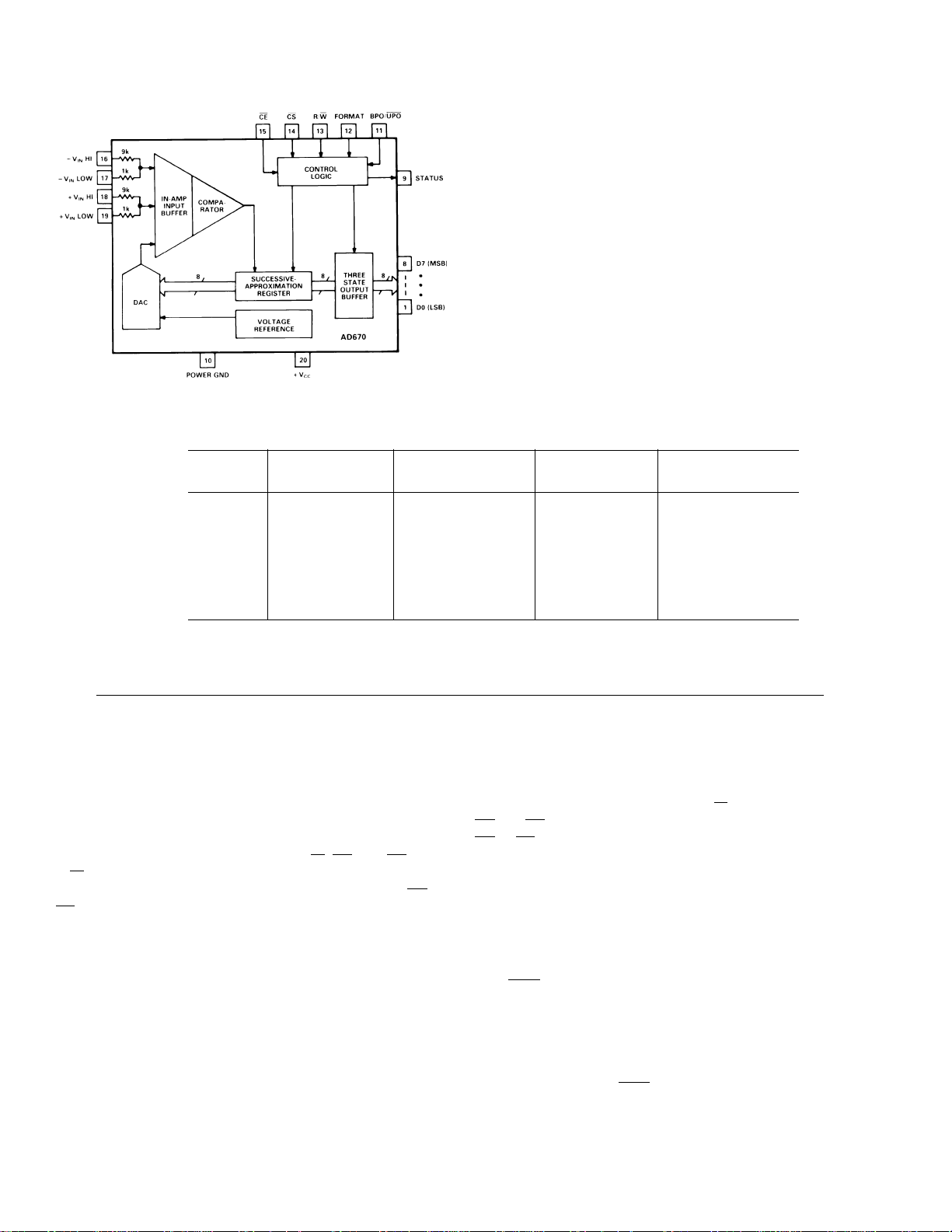
Figure 1. AD670 Block Diagram and Terminal
Configuration (AII Packages)
ABSOLUTE MAXIMUM RATINGS*
V
CC
to Ground . . . . . . . . . . . . . . . . . . . . . . . . . . . 0 V to +7.5 V
Digital Inputs (Pins 11–15) . . . . . . . . . . . –0.5 V to V
CC
+0.5 V
Digital Outputs (Pins 1–9) . Momentary Short to V
CC
or Ground
Analog Inputs (Pins 16–19) . . . . . . . . . . . . . . . –30 V to +30 V
Power Dissipation . . . . . . . . . . . . . . . . . . . . . . . . . . . . 450 mW
Storage Temperature Range . . . . . . . . . . . . . –65°C to +150°C
Lead Temperature (Soldering, 10 sec) . . . . . . . . . . . . . +300°C
*Stresses above those listed under “Absolute Maximum Ratings” may cause
permanent damage to the device. This is a stress rating only and functional
operation of the device at them or any other conditions above those indicated in
the operational sections of this specification is not implied. Exposure to absolute
maximum rating conditions for extended periods may affect device reliability.
CIRCUIT OPERATION/FUNCTIONAL DESCRIPTION
The AD670 is a functionally complete 8-bit signal conditioning
A/D converter with microprocessor compatibility. The input
section uses an instrumentation amplifier to accomplish the
voltage to current conversion. This front end provides a high
impedance, low bias current differential amplifier. The com-
mon-mode range allows the user to directly interface the device
to a variety of transducers.
The AID conversions are controlled by R/
W, CS, and CE. The
R/
W line directs the converter to read or start a conversion. A
minimum write/start pulse of 300 ns is required on either
CE or
CS. The STATUS line goes high, indicating that a conversion is
in process. The conversion thus begun, the internal 8-bit DAC
is sequenced from MSB to LSB using a novel successive ap-
proximation technique. In conventional designs, the DAC is
stepped through the bits by a clock. This can be thought of as a
static design since the speed at which the DAC is sequenced is
determined solely by the clock. No clock is used in the AD670.
Instead, a “dynamic SAR” is created consisting of a string of in-
verters with taps along the delay line. Sections of the delay line
between taps act as one shots. The pulses are used to set and re-
set the DAC’s bits and strobe the comparator. When strobed,
the comparator then determines whether the addition of each
successively weighted bit current causes the DAC current sum
to be greater or less than the input current. If the sum is less,
the bit is turned off. After all bits are tested, the SAR holds an
8-bit code representing the input signal to within 1/2 LSB
accuracy. Ease of implementation and reduced dependence on
process related variables make this an attractive approach to a
successive approximation design.
The SAR provides an end-of-conversion signal to the control
logic which then brings the STATUS line low. Data outputs re-
main in a high impedance state until R/
W is brought high with
CE and CS low and allows the converter to be read. Bringing
CE or CS high during the valid data period ends the read cycle.
The output buffers cannot be enabled during a conversion. Any
convert start commands will be ignored until the conversion
cycle is completed; once a conversion cycle has been started it
cannot be stopped or restarted.
The AD670 provides the user with a great deal of flexibility by
offering two input spans and formats and a choice of output
codes. Input format and input range can each be selected. The
BPO/
UPO pin controls a switch which injects a bipolar offset
current of a value equal to the MSB less 1/2 LSB into the sum-
ming node of the comparator to offset the DAC output. Two
precision 10 to 1 attenuators are included on board to provide
input range selection of 0 V to 2.55 V or 0 mV to 255 mV. Ad-
ditional ranges of –1.28 V to 1.27 V and –128 mV to 127 mV
are possible if the BPO/
UPO switch is high when the conversion
is started. Finally, output coding can be chosen using the FOR-
MAT pin when the conversion is started. In the bipolar mode
and with a Logic 1 on FORMAT, the output is in two’s comple-
ment; with a Logic 0, the output is offset binary.
Loading...