


 Loading...
a |
CMOS |
|
DDS Modulator |
||
|
|
AD7008 |
|
|
|
FEATURES
Single +5 V Supply
32-Bit Phase Accumulator
On-Chip COSINE and SINE Look-Up Tables
On-Chip 10-Bit DAC
Frequency, Phase and Amplitude Modulation
Parallel and Serial Loading
Software and Hardware Power Down Options
20 MHz and 50 MHz Speed Grades
44-Pin PLCC
APPLICATIONS
Frequency Synthesizers
Frequency, Phase or Amplitude Modulators
DDS Tuning
Digital Modulation
PRODUCT DESCRIPTION
The AD7008 direct digital synthesis chip is a numerically controlled oscillator employing a 32-bit phase accumulator, sine and cosine look-up tables and a 10-bit D/A converter integrated on a single CMOS chip. Modulation capabilities are provided for
phase modulation, frequency modulation, and both in-phase and quadrature amplitude modulation suitable for QAM and SSB generation.
Clock rates up to 20 MHz and 50 MHz are supported. Frequency accuracy can be controlled to one part in 4 billion. Modulation may be effected by loading registers either through the parallel microprocessor interface or the serial interface. A frequency-select pin permits selection between two frequencies on a per cycle basis.
The serial and parallel interfaces may be operated independently and asynchronously from the DDS clock; the transfer control signals are internally synchronized to prevent metastability problems. The synchronizer can be bypassed to reduce the transfer latency in the event that the microprocessor clock is synchronous with the DDS clock.
A power-down pin allows external control of a power-down mode (also accessible through the microprocessor interface) The AD7008 is available in 44-pin PLCC.
PRODUCT HIGHLIGHT
1.Low Power
2.DSP/μP Interface
3.Completely Integrated
FUNCTIONAL BLOCK DIAGRAM
VAA |
|
GND |
|
|
|
|
|
|
|
|
|
FS ADJUST |
VREF |
|
CLOCK |
|
|
|
|
|
|
|
|
IQMOD [19:10] |
|
|
|
|
|
|
|
|
|
|
|
|
|
|
|
|
|
|
||
|
|
|
|
|
|
|
|
|
10 |
|
|
FULLSCALE |
||
FSELECT |
|
|
|
|
|
|
|
|
|
|
ADJUST |
COMP |
||
|
|
|
|
|
|
|
|
10 |
|
|
||||
|
32 |
|
32 |
|
|
|
|
|
10 |
|
|
|
|
|
FREQ0 |
|
|
|
|
|
|
|
|
|
|
|
|
||
|
|
|
|
|
|
SIN |
|
|
|
|
|
|
||
|
|
|
|
|
|
|
|
|
|
|
|
|
||
REG |
|
|
|
|
|
|
|
|
|
|
|
|
|
|
32 |
|
|
12 |
|
12 |
|
|
|
Σ |
10 |
|
IOUT |
||
|
|
Σ |
Σ |
|
|
|
|
|||||||
|
|
|
SIN/COS |
|
|
|
|
|||||||
|
MUX |
|
|
|
|
|
|
10-BIT DAC |
||||||
|
|
|
|
|
ROM |
10 |
|
|||||||
|
32 |
|
|
|
|
|
|
|
10 |
|
|
|
IOUT |
|
|
|
|
|
|
|
|
|
|
|
|
|
|
|
|
FREQ1 |
|
|
PHASE |
|
12 |
|
|
COS |
|
|
|
|
|
|
REG |
|
ACCUMULATOR |
|
|
|
|
|
|
|
|
|
|||
|
|
|
|
|
|
|
|
|
10 |
|
|
|
|
|
|
|
|
|
|
PHASE REG |
|
|
IQMOD [9:0] |
|
|
|
|
||
SCLK |
|
|
|
|
|
|
|
|
|
|
|
|
|
|
32-BIT SERIAL REGISTER |
|
|
|
|
|
|
|
|
|
|
|
|
||
SDATA |
|
|
|
|
|
|
|
|
|
|
|
|
|
|
32-BIT PARALLEL REGISTER |
COMMAND REG |
|
|
|
|
|
AD7008 |
|
|
|||||
|
|
|
|
|
|
|
|
|||||||
|
MPU INTERFACE |
|
|
|
|
TRANSFER LOGIC |
|
|
|
|
|
|||
D0 |
|
D15 |
WR |
CS |
|
|
TC0 |
TC3 |
LOAD |
TEST |
RESET |
|
SLEEP |
|
REV. B
Information furnished by Analog Devices is believed to be accurate and reliable. However, no responsibility is assumed by Analog Devices for its use, nor for any infringements of patents or other rights of third parties which may result from its use. No license is granted by implication or otherwise under any patent or patent rights of Analog Devices.
© Analog Devices, Inc., 1995
One Technology Way, P.O. Box 9106, Norwood. MA 02062-9106, U.S.A. Tel: 617/329-4700 Fax: 617/326-8703
|
1 (VAA = VDD = +5 V ± 5%; TA = TMIN to TMAX, RSET = 390 Ω, RLOAD = 1 Ω for |
||||||||
AD7008–SPECIFICATIONS |
IOUT and |
|
, unless otherwise noted) |
|
|
|
|||
IOUT |
|
|
|
||||||
|
AD7008AP20 |
|
|
|
AD7008JP50 |
|
|
Test Conditions/ |
|
Parameter |
Min |
Typ |
Max |
Min |
Typ |
Max |
Units |
Comments |
|
SIGNAL DAC SPECIFICATIONS |
|
|
|
|
|
|
|
|
|
Resolution |
10 |
|
|
|
10 |
|
|
Bits |
|
Update Rate (fMAX) |
|
|
20 |
|
|
|
50 |
MSPS |
|
IOUT Full Scale |
|
20 |
|
|
|
20 |
|
mA |
|
Output Compliance |
|
|
1 |
|
|
|
1 |
Volts |
|
DC Accuracy |
|
|
|
|
|
|
|
|
|
Integral Nonlinearity |
|
+1 |
|
|
|
+1 |
|
LSB |
|
Differential Nonlinearity |
|
±1 |
|
|
|
±1 |
|
LSB |
|
DDS SPECIFICATIONS2 |
|
|
|
|
|
|
|
|
|
Update Rate (fMAX) |
|
|
20 |
|
|
|
50 |
MSPS |
|
Dynamic Specifications |
|
|
|
|
|
|
|
|
|
Signal-to-Noise |
50 |
|
|
|
50 |
|
|
dB |
fCLK = fMAX, |
|
|
|
|
|
|
|
|
|
fOUT = 2 MHz |
Total Harmonic Distortion |
–55 |
|
|
|
–53 |
|
|
dB |
fCLK = fMAX, |
Spurious Free Dynamic Range (SFDR)3 |
|
|
|
|
|
|
|
|
fOUT = 2 MHz |
|
|
|
|
|
|
|
|
|
|
Narrow Band (±50 kHz) |
–70 |
|
|
|
–70 |
|
|
dBc |
fCLK = 6.25 MHz, |
Wide Band (±2 MHz) |
–55 |
|
|
|
–55 |
|
|
dBc |
fOUT = 2.11 MHz |
|
|
|
|
|
|
||||
VOLTAGE REFERENCE |
|
|
|
|
|
|
|
|
|
Internal Reference @ +25°C4 |
1.2 |
1.27 |
1.35 |
|
1.2 |
1.27 |
1.35 |
Volts |
|
Reference TC |
|
300 |
|
|
|
300 |
|
ppm/°C |
|
VREF Overdrive5 |
0 |
2 |
|
|
0 |
2 |
|
V |
|
LOGIC INPUTS |
|
|
|
|
|
|
|
|
|
VINH, Input High Voltage |
VDD–0.9 |
|
|
|
VDD–0.9 |
|
|
Volts |
|
VINL, Input Low Voltage |
|
|
0.9 |
|
|
|
0.9 |
Volts |
|
IINH, Input Current |
|
|
10 |
|
|
|
10 |
μA |
|
CIN, Input Capacitance |
|
|
10 |
|
|
|
10 |
pF |
|
POWER SUPPLIES |
|
|
|
|
|
|
|
|
|
VDD |
4.75 |
|
5.25 |
|
4.75 |
|
5.25 |
Volts |
RSET = 390 Ω |
IAA |
|
26 |
|
|
|
26 |
|
mA |
|
IDD |
|
22 + 1.5/MHz |
|
22 + 1.5/MHz |
|
mA |
|
||
IAA + IDD |
|
|
|
|
|
|
|
|
|
fCLK = Max |
|
80 |
110 |
|
|
125 |
160 |
mA |
|
Sleep = VDD |
|
|
10 |
|
|
|
20 |
mA |
|
NOTES
1Operating temperature ranges as follows: A Version: –40°C to +85°C; J Version: 0°C to +70°C. 2All dynamic specifications are measured using IOUT. 100% Production tested.
3fCLK = 6.25 MHz, Frequency Word = 5671C71C HEX, fOUT = 2.11 MHz.
4VREF may be externally driven between 0 and VDD.
5Do not allow reference current to cause power dissipation beyond the limit of I AA + IDD shown above. Specifications subject to change without notice.
–2– |
REV. B |

|
|
|
|
|
|
|
|
|
|
|
|
|
|
|
|
AD7008 |
|
|
|
|
|
|
|
|
|
|
|
|
|
|
|
||||
TIMING CHARACTERISTICS (VAA = VDD +5 V ± 5%; TA = TMIN to TMAX, unless otherwise noted) |
|
||||||||||||||||
|
|
|
|
|
|
|
|
|
|
|
|
|
|
|
|
||
|
|
AD7008AP20 |
|
AD7008JP50 |
|
|
|
|
|
|
|
|
|
|
|
||
Parameter |
Min |
Typ |
Max |
Min |
Typ |
Max |
Units |
Test Conditions/Comments |
|
||||||||
|
|
|
|
|
|
|
|
|
|
|
|
|
|
|
|
|
|
t1 |
50 |
|
|
20 |
|
|
ns |
CLOCK Period |
|
||||||||
t2 |
20 |
|
|
8 |
|
|
ns |
|
|
CLOCK High Duration |
|
||||||
t3 |
20 |
|
|
8 |
|
|
ns |
|
|
CLOCK Low Duration |
|
||||||
t4 |
5 |
|
|
5 |
|
|
ns |
CLOCK to Control Setup Time |
|
||||||||
t5 |
3 |
|
|
3 |
|
|
ns |
CLOCK to Control Hold Time |
|
||||||||
t6 |
4t1 |
|
|
4t1 |
|
|
ns |
LOAD Period |
|
||||||||
t7 |
2t1 |
|
|
2t1 |
|
|
ns |
LOAD High Duration1 |
|
||||||||
t8 |
5 |
|
|
5 |
|
|
ns |
LOAD High to TC0–TC3 Setup Time |
|
||||||||
t9 |
5 |
|
|
5 |
|
|
ns |
LOAD High to TC0–TC3 Hold Time |
|
||||||||
t10 |
10 |
|
|
10 |
|
|
ns |
|
WR |
Falling to |
CS |
Low Setup Time |
|
||||
t11 |
10 |
|
|
10 |
|
|
ns |
|
WR |
Falling to |
CS |
Low Hold Time |
|
||||
t12 |
20 |
|
|
20 |
|
|
ns |
|
Minimum |
WR |
Low Duration |
|
|||||
t13 |
10 |
|
|
10 |
|
|
ns |
|
Minimum |
WR |
High Duration |
|
|||||
t14 |
3 |
|
|
3 |
|
|
ns |
|
|
WR |
to D0–D15 Setup Time |
|
|||||
t15 |
3 |
|
|
3 |
|
|
ns |
|
WR |
to D0–D15 Hold Time |
|
||||||
t16 |
20 |
|
|
20 |
|
|
ns |
SCLK Period |
|
||||||||
t17 |
8 |
|
|
8 |
|
|
ns |
SCLK High Duration |
|
||||||||
t18 |
8 |
|
|
8 |
|
|
ns |
SCLK Low Duration |
|
||||||||
t19 |
10 |
|
|
10 |
|
|
ns |
SCLK Rising to SDATA Setup Time |
|
||||||||
t20 |
10 |
|
|
10 |
|
|
ns |
SCLK Rising to SDATA Hold Time |
|
||||||||
NOTE
1May be reduced to 1t1 if LOAD is synchronized to CLOCK and Setup (t4) and Hold (t5) Times for LOAD to CLOCK are observed.
|
|
t1 |
|
CS |
|
|
|
|
|
t2 |
|
|
|
|
|
|
|
|
|
|
|
|
|
CLOCK |
|
|
|
|
t10 |
t11 |
|
|
|
|
|
|
|
|
|
|
|
|
t3 |
WR |
|
|
|
|
t4 |
|
|
|
|
t12 |
t13 |
FSEL, LOAD, |
VALID |
|
VALID |
|
t14 |
t15 |
|
TC3–TC0 |
|
|
|
|
|
||
|
|
|
D0–D15 |
VALID DATA |
|
||
|
t5 |
|
|
|
|||
|
|
|
|
|
|
|
|
Figure 1. Clock Synchronization Timing |
|
Figure 3. Parallel Port Timing |
|||||
|
|
|
|
|
|
|
t16 |
|
|
t |
6 |
|
|
|
t17 |
|
|
t7 |
|
SCLK |
|
|
|
|
LOAD |
|
|
|
|
t18 |
|
|
|
|
|
|
t20 |
|
|
|
|
|
|
|
|
|
|
|
t8 |
|
t9 |
|
t19 |
|
|
TC0–TC3 |
VALID |
|
SDATA |
DB31 |
|
DB0 |
|
|
Figure 2. Register Transfer Timing |
|
Figure 4. Serial Port Timing |
||||
REV. B |
–3– |
AD7008
ABSOLUTE MAXIMUM RATINGS*
(TA = +25°C unless otherwise noted)
VAA, VDD to GND . . . . . . . . . . . . . . . . . |
. . . . . . –0.3 V to +7 |
V |
AGND to DGND . . . . . . . . . . . . . . . . . . |
. . . –0.3 V to +0.3 V |
|
Digital I/O Voltage to DGND . . . . . . . . |
–0.3 V to VDD + 0.3 |
V |
Analog I/O Voltage to AGND . . . . . . . . |
–0.3 V to VDD + 0.3 |
V |
Operating Temperature Range |
–40°C to +85°C |
|
Industrial (A Version) . . . . . . . . . . . . . |
||
Commercial (J Version) . . . . . . . . . . . . |
. . . . . .0°C to +70°C |
|
Storage Temperature Range . . . . . . . . . . |
. . . –65°C to +150°C |
|
Lead Temperature (Soldering, 10 secs) . . |
. . . . . . . . . . +300°C |
|
Junction Temperature . . . . . . . . . . . . . . . |
. . . . . . . . . . +115°C |
|
PLCC θJA Thermal Impedance . . . . . . . . |
. . . . . . . +53.8°C/W |
|
θJC Thermal Impedance . . . . . . . . |
. . . . . . . +24.1°C/W |
|
*Stresses above those listed under “Absolute Maximum Ratings” may cause permanent damage to the device. This is a stress rating only and functional operation of the device at these or any other conditions above those listed in the operational sections of this specification is not implied. Exposure to absolute maximum rating conditions for extended periods may affect device reliability.
ORDERING GUIDE
|
Temperature |
Package |
Package |
Model |
Range |
Description |
Option |
|
|
|
|
AD7008AP20 |
–40°C to +85°C |
44-Pin PLCC |
P-44A |
AD7008JP50 |
0°C to +70°C |
44-Pin PLCC |
P-44A |
AD7008/PCB* |
|
1–3.5" Disk |
|
|
|
|
|
*AD7008/PCB DDS Evaluation Kit, assembled and tested. Kit includes an AD7008JP50.
|
|
32-BIT PARALLEL ASSEMBLY REGISTER |
|
|
|
|
|
|||||
|
|
|
|
|
|
|
|
|
|
|
|
|
|
MSB |
|
|
|
|
|
|
|
LSB |
|
|
|
|
|
|
|
|
|
|
|
|
|
|
D15–D0 ← A WORD* |
|
|
|
|
|
|
|
A WORD |
|
|
|
|||
|
|
|
|
|
|
|
|
|
|
D15–D0 ← B WORD |
||
|
|
A WORD |
|
B WORD |
|
|
|
|||||
|
|
|
|
|
|
|
|
|
|
|
|
|
*MOST SIGNIFICANT WORD IS LOADED FIRST |
|
|
|
|
|
|||||||
|
Figure 5. 16-Bit Parallel Port Loading Sequence |
|||||||||||
|
|
|
|
|
|
|||||||
|
|
|
32-BIT PARALLEL ASSEMBLY REGISTER |
|
|
|
||||||
MSB |
|
|
|
|
|
|
|
|
LSB |
|||
|
|
|
|
|
|
|
|
|||||
|
|
|
|
|
|
|
|
|
|
|
D7–D0 ← A BYTE* |
|
|
|
|
|
|
|
|
|
A BYTE |
|
|||
|
|
|
|
|
|
|
|
|
|
|
D7–D0 ← B BYTE |
|
|
|
|
|
|
|
A BYTE |
|
B BYTE |
|
|||
|
|
|
|
|
|
|
|
|
|
D7–D0 ← C BYTE |
||
|
|
|
|
A BYTE |
|
B BYTE |
|
C BYTE |
|
|||
|
|
|
|
|
|
|
|
|
D7–D0 ← D BYTE |
|||
|
A BYTE |
|
B BYTE |
|
C BYTE |
|
D BYTE |
|
||||
|
|
|
|
|
|
|
|
|
|
|
|
|
*MOST SIGNIFICANT BYTE IS LOADED FIRST
Figure 6. 8-Bit Parallel Port Loading Sequence
CAUTION
ESD (electrostatic discharge) sensitive device. Electrostatic charges as high as 4000 V readily accumulate on the human body and test equipment and can discharge without detection. Although the AD7008 features proprietary ESD protection circuitry, permanent damage may occur on devices subjected to high energy electrostatic discharges. Therefore, proper ESD precautions are recommended to avoid performance degradation or loss of functionality.
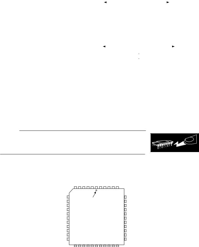
PIN CONFIGURATION
PLCC
|
V |
COMP |
FSADJUST |
V |
IOUT |
IOUT |
AGND |
DGND |
SDATA |
SCLK |
TEST |
|
|
REF |
|
|
AA |
|
|
|
|
|
|
|
|
|
6 |
|
|
|
|
|
|
|
|
|
40 |
|
|
|
|
|
|
|
|
|
|
|
|
|
|
DGND |
7 |
|
|
PIN NO. 1 IDENTIFIER |
|
39 |
VDD |
|||||
D8 |
|
|
|
|
|
RESET |
||||||
|
|
|
|
|
|
|
|
|
|
|
||
D9 |
|
|
|
|
|
|
|
|
|
|
|
SLEEP |
D10 |
|
|
|
|
|
|
|
|
|
|
|
LOAD |
D11 |
|
|
|
AD7008 PLCC |
|
|
|
TC3 |
||||
D12 |
|
|
|
|
TOP VIEW |
|
|
|
|
TC2 |
||
D13 |
|
|
|
(NOT TO SCALE) |
|
|
|
TC1 |
||||
|
|
|
|
|
|
|
|
|
|
|
||
D14 |
|
|
|
|
|
|
|
|
|
|
|
TC0 |
D15 |
|
|
|
|
|
|
|
|
|
|
|
FSELECT |
WR |
|
|
|
|
|
|
|
|
|
|
|
CLOCK |
VDD |
17 |
|
|
|
|
|
|
|
|
|
29 |
DGND |
|
18 |
|
|
|
|
|
|
|
|
|
28 |
|
|
DGND |
D0 |
D1 |
D2 |
D3 |
D4 |
D5 |
D6 |
D7 |
CS |
DD |
|
|
V |
|
||||||||||
WARNING!
ESD SENSITIVE DEVICE
–4– |
REV. B |

|
AD7008 |
|
|
|
|
|
PIN DESCRIPTION |
|
|
|
|
Mnemonic |
Function |
|
|
|
|
POWER SUPPLY |
||
VAA |
Positive power supply for the analog section. A 0.1 μF decoupling capacitor should be connected between VAA and |
|
|
AGND. This is +5 V ± 5%. |
|
AGND |
Analog Ground. |
|
VDD |
Positive power supply for the digital section. A 0.1 μF decoupling capacitor should be connected between VDD |
|
|
and DGND. This is +5 V ± 5%. Both VAA and VDD should be externally tied together. |
|
DGND |
Digital Ground; both AGND and DGND should be externally tied together. |
|
ANALOG SIGNAL AND REFERENCE
IOUT, IOUT |
Current Output. This is a high impedance current source. A load resistor should be connected between IOUT |
||
|
and AGND. |
IOUT |
should be either tied directly to AGND or through an external load resistor to AGND. |
FS ADJUST |
Full-Scale Adjust Control. A resistor (RSET) is connected between this pin and AGND. This determines the mag- |
||
|
nitude of the full-scale DAC current. The relationship between RSET and the full-scale current is as follows: |
||
|
|
|
|
6233 ×VREF |
|||||
|
|
|
IOUTFULL-SCALE (mA) = |
|
VREF = 1.27 V nominal RSET = 390 Ω typical |
||||
|
|
|
|
||||||
|
|
|
|
RSET |
|||||
VREF |
Voltage Reference Input. A 0.1 μF decoupling ceramic capacitor should be connected between VREF and VAA. |
||||||||
|
|
|
There is an internal 1.27 volt reference which can be overdriven by an external reference if required. See |
||||||
|
|
|
specifications for maximum range. |
|
|
|
|
|
|
COMP |
Compensation pin. This is a compensation pin for the internal reference amplifier. A 0.1 μF decoupling ceramic |
||||||||
|
|
|
capacitor should be connected between COMP and VAA. |
||||||
DIGITAL INTERFACE AND CONTROL |
|
|
|
|
|
|
|||
CLOCK |
Digital Clock Input for DAC and NCO. DDS output frequencies are expressed as a binary fraction of the fre- |
||||||||
|
|
|
quency of this clock. The output frequency accuracy and phase noise is determined by this clock. |
||||||
FSELECT |
Frequency Select Input. FSELECT controls which frequency register, FREQ0 or FREQ1, is used in the phase |
||||||||
|
|
|
accumulator. Frequency selection can be done on a cycle-per-cycle basis. See Tables I, II and III. |
||||||
LOAD |
Register load, active high digital Input. This pin, in conjunction with TC3–TC0, control loading of internal regis- |
||||||||
|
|
|
ters from either the parallel or serial assembly registers. The load pin must be high at least 1t1. See Table II. |
||||||
TC3–TC0 |
Transfer Control address bus, digital inputs. This address determines the source and destination registers that are |
||||||||
|
|
|
used during a transfer. The source register can either be the parallel assembly register or the serial assembly regis- |
||||||
|
|
|
ter. The destination register can be any of the following: COMMAND REG, FREQ0 REG, FREQ1 REG, |
||||||
|
|
|
PHASE REG or IQMOD REG. TC3–TC0 should be valid prior to LOAD rising and should not change until |
||||||
|
|
|
LOAD falls. The Command Register can only be loaded from the parallel assembly register. See Table II. |
||||||
|
|
|
Chip Select, active low digital input. This input in conjunction with |
|
is used when writing to the parallel |
||||
CS |
WR |
||||||||
|
|
|
assembly register. |
|
|
|
|
|
|
|
|
Write, active low digital input. This input in conjunction with |
|
is used when writing to the parallel assembly |
|||||
WR |
CS |
||||||||
|
|
|
register. |
|
|
|
|
|
|
D7–D0 |
Data Bus, digital inputs. These represent the low byte of the 16-bit data input port used to write to the 32-bit |
||||||||
|
|
|
parallel assembly register. The databus can configured for either a 8-bit or 16-bit MPU/DSP ports. |
||||||
D15–D8 |
Data Bus, digital inputs. These represent the high byte of the 16-bit data input port used to write to the 32-bit |
||||||||
|
|
|
parallel assembly register. The databus can be configured for either a 8-bit or 16-bit MPU/DSP ports. When the |
||||||
|
|
|
databus is configured for 8-bit operation, D8–D15 should be tied to DGND. |
||||||
SCLK |
Serial Clock, digital input. SCLK is used, in conjunction with SDATA, to clock data into the 32-bit serial assem- |
||||||||
|
|
|
bly register. |
|
|
|
|
|
|
SDATA |
Serial Data, digital input. Serial data is clocked on the rising edge of SCLK, Most Significant Bit (MSB) first. |
||||||||
SLEEP |
Low power sleep control, active high digital input. SLEEP puts the AD7008 into a low power sleep mode. Inter- |
||||||||
|
|
|
nal clocks are disabled, while also turning off the DAC current sources. A SLEEP bit is also provided in the |
||||||
|
|
|
COMMAND REG to put the AD7008 into a low power sleep mode. |
||||||
RESET |
Register Reset, active high digital input. RESET clears the COMMAND REG and all the modulation registers to |
||||||||
|
|
|
zero. |
|
|
|
|
|
|
TEST |
Test Mode. This is used for factory test only and should be left as a No Connect. |
||||||||
|
|
|
|
|
|
|
|
|
|
REV. B |
–5– |
Loading...