


 Loading...
a |
Loop-Powered 4–20 mA |
|
Sensor Transmitter |
||
|
|
|
|
|
AD693 |
|
|
|
|
FEATURES |
FUNCTIONAL BLOCK DIAGRAM |
|
Instrumentation Amplifier Front End |
|
|
Loop-Powered Operation |
|
|
Precalibrated 30 mV or 60 mV Input Spans |
|
|
Independently Adjustable Output Span and Zero |
|
|
Precalibrated Output Spans: 4–20 mA Unipolar |
|
|
0–20 mA Unipolar |
|
|
12 6 8 mA Bipolar |
|
|
Precalibrated 100 V RTD Interface |
|
|
6.2 V Reference with Up to 3.5 mA of Current Available |
|
|
Uncommitted Auxiliary Amp for Extra Flexibility |
|
|
Optional External Pass Transistor to Reduce |
|
|
Self-Heating Errors |
|
PRODUCT DESCRIPTION
The AD693 is a monolithic signal conditioning circuit which accepts low-level inputs from a variety of transducers to control a standard 4–20 mA, two-wire current loop. An on-chip voltage reference and auxiliary amplifier are provided for transducer excitation; up to 3.5 mA of excitation current is available when the device is operated in the loop-powered mode. Alternatively, the device may be locally powered for three-wire applications when 0–20 mA operation is desired.
Precalibrated 30 mV and 60 mV input spans may be set by simple pin strapping. Other spans from 1 mV to 100 mV may be realized with the addition of external resistors. The auxiliary amplifier may be used in combination with on-chip voltages to provide six precalibrated ranges for 100 Ω RTDs. Output span and zero are also determined by pin strapping to obtain the standard ranges: 4–20mA, 12 ± 8 mA and 0–20 mA.
Active laser trimming of the AD693’s thin-film resistors result in high levels of accuracy without the need for additional adjustments and calibration. Total unadjusted error is tested on every device to be less than 0.5% of full scale at +25°C, and less than 0.75% over the industrial temperature range. Residual nonlinearity is under 0.05%. The AD693 also allows for the use of an external pass transistor to further reduce errors caused by self-heating.
For transmission of low-level signals from RTDs, bridges and pressure transducers, the AD693 offers a cost-effective signal conditioning solution. It is recommended as a replacement for discrete designs in a variety of applications in process control, factory automation and system monitoring.
The AD693 is packaged in a 20-pin ceramic side-brazed DIP, 20-pin Cerdip, and 20-pin LCCC and is specified over the –40°C to +85°C industrial temperature range.
REV. A
Information furnished by Analog Devices is believed to be accurate and reliable. However, no responsibility is assumed by Analog Devices for its use, nor for any infringements of patents or other rights of third parties which may result from its use. No license is granted by implication or otherwise under any patent or patent rights of Analog Devices.
PRODUCT HIGHLIGHTS
1.The AD693 is a complete monolithic low-level voltage-to- current loop signal conditioner.
2.Precalibrated output zero and span options include
4–20 mA, 0–20 mA, and 12 ± 8 mA in twoand three-wire configurations.
3.Simple resistor programming adds a continuum of ranges to the basic 30 mV and 60 mV input spans.
4.The common-mode range of the signal amplifier input extends from ground to near the device’s operating voltage.
5.Provision for transducer excitation includes a 6.2 V reference output and an auxiliary amplifier which may be configured for voltage or current output and signal amplification.
6.The circuit configuration permits simple linearization of bridge, RTD, and other transducer signals.
7.A monitored output is provided to drive an external pass transistor. This feature off-loads power dissipation to extend the temperature range of operation, enhance reliability, and minimize self-heating errors.
8.Laser-wafer trimming results in low unadjusted errors and affords precalibrated input and output spans.
9.Zero and span are independently adjustable and noninteractive to accommodate transducers or user defined ranges.
10.Six precalibrated temperature ranges are available with a 100 Ω RTD via pin strapping.
One Technology Way, P.O. Box 9106, Norwood, MA 02062-9106, U.S.A. Tel: 617/329-4700 Fax: 617/326-8703
|
|
(@ +258C and VS = +24 V. Input Span = 30 mV or 60 mV. Output Span = 4–20 mA, |
||||
AD693–SPECIFICATIONS RL = 250 V, VCM = 3.1 V, with external pass transistor unless otherwise noted.) |
||||||
|
Model |
|
AD693AD/AQ/AE |
|
||
|
|
Conditions |
Min |
Typ |
Max |
Units |
|
|
|
|
|
|
|
|
LOOP-POWERED OPERATION |
|
|
|
|
|
|
|
|
|
|
|
|
|
TOTAL UNADJUSTED ERROR1, 2 |
|
|
±0.25 |
60.5 |
% Full Scale |
|
TMIN to TMAX |
|
|
±0.4 |
60.75 |
% Full Scale |
|
100 Ω RTD CALIBRATION ERROR3 |
(See Figure 17) |
|
±0.5 |
±2.0 |
°C |
|
LOOP POWERED OPERATION2 |
|
|
±25 |
|
μA |
|
Zero Current Error4 |
Zero = 4 mA |
|
680 |
||
|
|
Zero = 12 mA |
|
±40 |
6120 |
μA |
|
|
Zero = 0 mA5 |
+7 |
+35 |
+100 |
μA |
|
vs. Temp. |
Zero = 4 mA |
|
±0.5 |
±1.5 |
μA/°C |
|
Power Supply Rejection (RTI) |
12 V ≤ VOP ≤ 36V6 |
|
±3.0 |
65.6 |
μV/V |
|
|
0 V ≤ VCM ≤ 6.2 V |
|
|
+VOP – 4 V6 |
|
|
Common-Mode Input Range |
(See Figure 3) |
0 |
|
V |
|
|
Common-Mode Rejection (RTI) |
0 V ≤ VCM ≤ 6.2 V |
|
±10 |
630 |
μV/V |
|
Input Bias Current7 |
|
|
+5 |
+20 |
nA |
|
TMIN to TMAX |
|
|
+7 |
+25 |
nA |
|
Input Offset Current7 |
VSIG = 0 |
|
±0.5 |
63.0 |
nA |
|
Transconductance |
|
|
|
|
|
|
Nominal |
30 mV Input Span |
|
0.5333 |
|
A/V |
|
|
60 mV Input Span |
|
0.2666 |
|
A/V |
|
Unadjusted Error |
0 V ≤ VCM ≤ 6.2 V |
|
±0.05 |
60.2 |
% |
|
vs. Common-Mode |
|
±0.03 |
±0.04 |
|
|
|
|
30 mV Input Span |
|
%/V |
||
|
|
60 mV Input Span |
|
±0.05 |
±0.06 |
%/V |
|
Error vs. Temp. |
|
|
±20 |
±50 |
ppm/°C |
|
Nonlinearity8 |
30 mV Input Span |
|
±0.01 |
60.05 |
% of Span |
|
|
60 mV Input Span |
|
±0.02 |
60.07 |
% of Span |
|
OPERATIONAL VOLTAGE RANGE |
|
|
|
|
|
|
Operational Voltage, VOP6 |
|
+12 |
|
+36 |
V |
|
Quiescent Current |
Into Pin 9 |
|
+500 |
+700 |
μA |
|
OUTPUT CURRENT LIMIT |
|
+21 |
+25 |
+32 |
mA |
|
|
|
|
|
|
|
|
COMPONENTS OF ERROR |
|
|
|
|
|
|
|
|
|
|
|
|
|
SIGNAL AMPLIFIER9 |
|
|
±40 |
|
μV |
|
Input Voltage Offset |
|
|
6200 |
||
|
vs. Temp |
12 V ≤ VOP ≤ 36 V6 |
|
±1.0 |
±2.5 |
μV/°C |
|
Power Supply Rejection |
|
±3.0 |
65.6 |
μV/V |
|
|
|
0 V ≤ VCM ≤ 6.2 V |
|
|
|
|
|
V/I CONVERTER9, 10 |
|
|
±30 |
±80 |
μA |
|
Zero Current Error |
Output Span = 4–20 mA |
|
|||
|
Power Supply Rejection |
12 V ≤ VOP ≤ 36 V6 |
|
±1.0 |
±3.0 |
μA/V |
|
Transconductance |
|
|
|
|
|
|
Nominal |
|
|
0.2666 |
±0.2 |
A/V |
|
Unadjusted Error |
|
|
±0.05 |
% |
|
|
6.200 V REFERENCE9, 12 |
|
|
±3 |
|
|
|
Output Voltage Tolerance |
|
|
612 |
mV |
|
|
vs. Temp. |
12 V ≤ VOP ≤ 36 V6 |
|
±20 |
±50 |
ppm/°C |
|
Line Regulation |
|
±200 |
6300 |
μV/V |
|
|
Load Regulation11 |
0 mA ≤ IREF ≤ 3 mA |
|
±0.3 |
60.75 |
mV/mA |
|
Output Current13 |
Loop Powered, (Figure 10) |
+3.0 |
+3.5 |
|
mA |
|
|
3-Wire Mode, (Figure 15) |
|
+5.0 |
|
mA |
|
|
|
|
|
|
|
–2– |
REV. A |
|
|
|
|
|
AD693 |
|
|
|
|
|
|
Model |
|
|
AD693AD |
|
|
|
Conditions |
Min |
Typ |
Max |
Units |
|
|
|
|
|
|
AUXILIARY AMPLIFIER |
|
|
|
+VOP – 4 V6 |
|
Common-Mode Range |
|
0 |
±50 |
V |
|
Input Offset Voltage |
|
|
±200 |
μV |
|
Input Bias Current |
|
|
+5 |
+20 |
nA |
Input Offset Current |
|
|
+0.5 |
±3.0 |
nA |
Common-Mode Rejection |
|
|
90 |
|
dB |
Power Supply Rejection |
|
|
105 |
|
dB |
Output Current Range |
Pin IX OUT |
+0.01 |
±0.005 |
+5 |
mA |
Output Current Error |
Pin VX – Pin IX |
|
|
% |
|
TEMPERATURE RANGE |
|
|
|
|
°C |
Case Operating14 |
TMIN to TMAX |
–40 |
|
+85 |
|
Storage |
|
–65 |
|
+150 |
°C |
NOTES
1Total error can be significantly reduced (typically less than 0.1%) by trimming the zero current. The remaining unadjusted error sources are transconductance and nonlinearity.
2The AD693 is tested as a loop powered device with the signal amp, V/I converter, voltage reference, and application voltages operating together. Specifications are valid for preset spans and spans between 30 mV and 60 mV.
3Error from ideal output assuming a perfect 100 Ω RTD at 0 and +100°C.
4Refer to the Error Analysis to calculate zero current error for input spans less than 30 mV.
5By forcing the differential signal amplifier input sufficiently negative the 7 μA zero current can always be achieved.
6The operational voltage (VOP) is the voltage directly across the AD693 (Pin 10 to 6 in two-wire mode, Pin 9 to 6 in local power mode). For example, VOP = VS –
(ILOOP × RL) in two-wire mode (refer to Figure 10).
7Bias currents are not symmetrical with input signal level and flow out of the input pins. The input bias current of the inverting input increases with input signal voltage, see Figure 2.
8Nonlinearity is defined as the deviation of the output from a straight line connecting the endpoints as the input is swept over a 30 mV and 60 mV input span.
9Specifications for the individual functional blocks are components of error that contribute to, and that are included in, the Loop Powered Operation specifications.
10Includes error contributions of V/I converter and Application Voltages.
11Changes in the reference output voltage due to load will affect the Zero Current. A 1% change in the voltage reference output will result in an error of 1% in the value of the Zero Current.
12If not used for external excitation, the reference should be loaded by approximately 1 mA (6.2 kΩ to common).
13In the loop powered mode up to 5 mA can be drawn from the reference, however, the lower limit of the output span will be increased accordingly. 3.5 mA is the maximum current the reference can source while still maintaining a 4 mA zero.
14The AD693 is tested with a pass transistor so TA TC.
Specifications subject to change without notice.
Specifications shown in boldface are tested on all production units at final electrical test. Results from those tests are used to calculate outgoing quality levels. All min and max specifications are guaranteed, although only those shown in boldface are tested on all production units.
ABSOLUTE MAXIMUM RATINGS
Supply Voltage . . . . . . . . . . . . . . . . . . . . . . . . . . . . . . . . +36 V Reverse Loop Current . . . . . . . . . . . . . . . . . . . . . . . . . 200 mA
Signal Amp Input Range . . . . . . . . . . . . . . . . . . –0.3 V to VOP Reference Short Circuit to Common . . . . . . . . . . . . Indefinite
Auxiliary Amp Input Voltage Range . . . . . . . . . . 0.3 V to VOP Auxiliary Amp Current Output . . . . . . . . . . . . . . . . . . . 10 mA Storage Temperature . . . . . . . . . . . . . . . . . . –65°C to +150°C Lead Temperature, 10 sec Soldering . . . . . . . . . . . . . +300°C Max Junction Temperature . . . . . . . . . . . . . . . . . . . . . +150°C
ORDERING GUIDE
|
Package |
Package |
Model |
Description |
Option |
|
|
|
AD693AD |
Ceramic Side-Brazed DIP |
D-20 |
AD693AQ |
Cerdip |
Q-20 |
AD693AE |
Leadless Ceramic Chip |
E-20A |
|
Carrier (LCCC) |
|
|
|
|
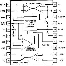
AD693 PIN CONFIGURATION
(AD, AQ, AE Packages)
Functional Diagram
REV. A |
–3– |
AD693–Typical Characteristics
Figure 1. Maximum Load Resistance vs. Power Supply
Figure 2. Differential Input Current vs. Input Signal Voltage Normalized to +IN
Figure 4. Bandwidth vs. Series Load Resistance
Figure 5. Signal Amplifier PSRR vs. Frequency
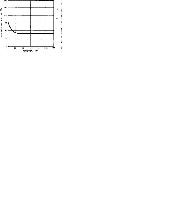
Figure 7. Input Current Noise vs. Frequency
Figure 8. Input Voltage Noise vs. Frequency
Figure 3. Maximum Common-Mode |
Figure 6. CMRR (RTI) vs. Frequency |
Voltage vs. Supply |
|
–4– |
REV. A |
Loading...