


AD676KN
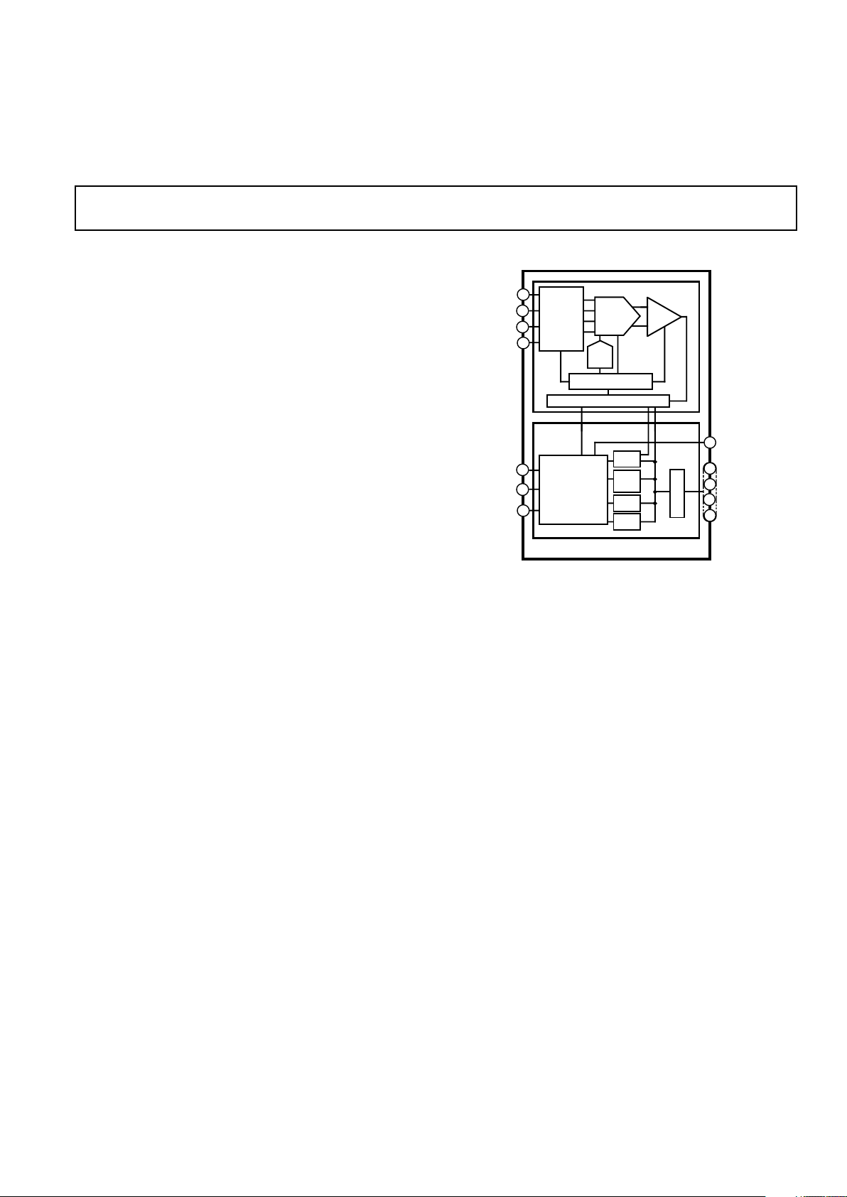
FUNCTIONAL BLOCK DIAGRAM
DIGITAL
CHIP
PAT
GEN
ALU
RAM
MICRO-CODED
CONTROLLER
AGND
AGND SENSE
CAL
SAMPLE
BUSY
COMP
ANALOG
CHIP
16-BIT
DAC
INPUT
BUFFERS
LOGIC & TIMING
CAL
DAC
LEVEL TRANSLATORS
16
BIT 1 – BIT 16
V
IN
V
REF
15
14
16
13
8
9
AD676
SAR
1
6
19
28
CLK 10
L
A
T
C
H
7
REV. A
Information furnished by Analog Devices is believed to be accurate and
reliable. However, no responsibility is assumed by Analog Devices for its
use, nor for any infringements of patents or other rights of third parties
which may result from its use. No license is granted by implication or
otherwise under any patent or patent rights of Analog Devices.
a
16-Bit 100 kSPS
Sampling ADC
AD676
FEATURES
Autocalibrating
On-Chip Sample-Hold Function
Parallel Output Format
16 Bits No Missing Codes
61 LSB INL
–97 dB THD
90 dB S/(N+D)
1 MHz Full Power Bandwidth
PRODUCT DESCRIPTION
The AD676 is a multipurpose 16-bit parallel output analog-to-
digital converter which utilizes a switched-capacitor/charge
redistribution architecture to achieve a 100 kSPS conversion
rate (10 µs total conversion time). Overall performance is opti-
mized by digitally correcting internal nonlinearities through
on-chip autocalibration.
The AD676 circuitry is segmented onto two monolithic chips—
a digital control chip fabricated on Analog Devices DSP CMOS
process and an analog ADC chip fabricated on our BiMOS II
process. Both chips are contained in a single package.
The AD676 is specified for ac (or “dynamic”) parameters such
as S/(N+D) Ratio, THD and IMD which are important in sig-
nal processing applications. In addition, dc parameters are
specified which are important in measurement applications.
One Technology Way, P.O. Box 9106, Norwood, MA 02062-9106, U.S.A.
Tel: 617/329-4700 Fax: 617/326-8703
The AD676 operates from +5 V and ± 12 V supplies and typi-
cally consumes 360 mW during conversion. The digital supply
(V
DD
) is separated from the analog supplies (V
CC
, V
EE
) for re-
duced digital crosstalk. An analog ground sense is provided for
the analog input. Separate analog and digital grounds are also
provided.
The AD676 is available in a 28-pin plastic DIP or 28-pin side-
brazed ceramic package. A serial-output version, the AD677, is
available in a 16-pin 300 mil wide ceramic or plastic package.

AD676–SPECIFICATIONS
AC SPECIFICATIONS
AD676J/A AD676K/B
Parameter Min Typ Max Min Typ Max Units
Total Harmonic Distortion (THD)
2
@ 83 kSPS, T
MIN
to T
MAX
–96 –88 –97 –90 dB
0.0016 0.004 0.0014 0.003 %
@ 100 kSPS, +25°C –96 –97 dB
0.0016 0.0014 %
@ 100 kSPS, T
MIN
to T
MAX
–92 –92 dB
0.0025 0.0025 %
Signal-to-Noise and Distortion Ratio (S/(N+D))
2, 3
@ 83 kSPS, T
MIN
to T
MAX
85 89 87 90 dB
@ 100 kSPS, +25°C8990dB
@ 100 kSPS, T
MIN
to T
MAX
86 86 dB
Peak Spurious or Peak Harmonic Component –98 –98 dB
Intermodulation Distortion (IMD)
4
2nd Order Products –102 –102 dB
3rd Order Products –98 –98 dB
Full Power Bandwidth 1 1 MHz
Noise 160 160 µV rms
DIGITAL SPECIFICATIONS
Parameter Test Conditions Min Typ Max Units
LOGIC INPUTS
V
IH
High Level Input Voltage 2.4 V
DD
+ 0.3 V
V
IL
Low Level Input Voltage –0.3 0.8 V
I
IH
High Level Input Current V
IH
= V
DD
–10 +10 µA
I
IL
Low Level Input Current V
IL
= 0 V –10 +10 µA
C
IN
Input Capacitance 10 pF
LOGIC OUTPUTS
V
OH
High Level Output Voltage I
OH
= 0.1 mA V
DD
–1 V V
I
OH
= 0.5 mA 2.4 V
V
OL
Low Level Output Voltage I
OL
= 1.6 mA 0.4 V
NOTES
1
V
REF
= 10.0 V, (Conversion Rate (fs) = 83 kSPS, f
IN
= 1.0 kHz, V
IN
= –0.05 dB, Bandwidth = fs/2 unless otherwise indicated. All measurements referred to a 0 dB
(20 V p-p) input signal. Values are post-calibration.
2
For other input amplitudes, refer to Figure 13.
3
For other input ranges/voltages reference values see Figure 12.
4
fa = 1008 Hz. fb = 1055 Hz. See Definition of Specifications section and Figure 15.
Specifications subject to change without notice.
(T
MIN
to T
MAX,
V
CC
= +12 V 6 5%, V
EE
= –12 V 6 5%, V
DD
= +5 V 6 10%)
1
(for all grades T
MIN
to T
MAX
, V
CC
= +12 V
6
5%, V
EE
= –12 V
6
5%, V
DD
= +5 V
6
10%)
REV. A
–2–

DC SPECIFICATIONS
AD676J/A AD676K/B
Parameter Min Typ Max Min Typ Max Units
TEMPERATURE RANGE
J, K Grades 0 +70 0 +70 °C
A, B Grades –40 +85 –40 +85 °C
ACCURACY
Resolution 16 16 Bits
Integral Nonlinearity (INL)
@ 83 kSPS, T
MIN
to T
MAX
±1 ±1 ±1.5 LSB
@ 100 kSPS, +25°C ±1 ±1 LSB
@ 100 kSPS, T
MIN
to T
MAX
±2 ±2 LSB
Differential Nonlinearity (DNL)–No Missing Codes 16 16 Bits
Bipolar Zero Error
2
(at Nominal Supplies) 0.005 0.005 % FSR
Gain Error (at Nominal Supplies)
@ 83 kSPS
2
0.005 0.005 % FSR
@ 100 kSPS, +25°C 0.005 0.005 % FSR
@ 100 kSPS
2
0.01 0.01 % FSR
Temperature Drift, Bipolar Zero
3
% FSR
J, K Grades 0.0015 0.0015 % FSR
A, B Grades 0.003 0.003 % FSR
Temperature Drift, Gain
3
J, K Grades 0.0015 0.0015 % FSR
A, B Grades 0.003 0.003 % FSR
VOLTAGE REFERENCE INPUT RANGE
4
(V
REF
)5 10 5 10V
ANALOG INPUT
5
Input Range (V
IN
) ±V
REF
±V
REF
V
Input Impedance * *
Input Settling Time 2 2 µs
Input Capacitance During Sample 50* 50* pF
Aperture Delay 6 6 ns
Aperture Jitter 100 100 ps
POWER SUPPLIES
Power Supply Rejection
V
CC
= +12 V ± 5% ±1 ±1 LSB
V
EE
= –12 V ± 5% ±1 ±1 LSB
V
DD
= +5 V ± 10% ±1 ±1 LSB
Operating Current
I
CC
14.5 18 14.5 18 mA
I
EE
14.5 18 14.5 18 mA
I
DD
25 25mA
Power Consumption 360 480 360 480 mW
NOTES
1
V
REF
= 5.0 V, Conversion Rate = 83 kSPS unless otherwise noted. Values are post-calibration.
2
Values shown apply to any temperature from T
MIN
to T
MAX
after calibration at that temperature.
3
Values shown are based upon calibration at +25°C with no additional calibration at temperature. Values shown are the worst case variation from the value at +25 °C.
4
See “APPLICATIONS” section for recommended voltage reference circuit, and Figure 12 for dynamic performance with other reference voltage values.
5
See “APPLICATIONS” section for recommended input buffer circuit.
*For explanation of input characteristics, see “ANALOG INPUT” section.
Specifications subject to change without notice.
(T
MIN
to T
MAX
, V
CC
= +12 V 6 5%, V
EE
= –12 V 6 5%, V
DD
= +5 V 6 1O%)
1
AD676
REV. A
–3–
AD676
REV. A
–4–
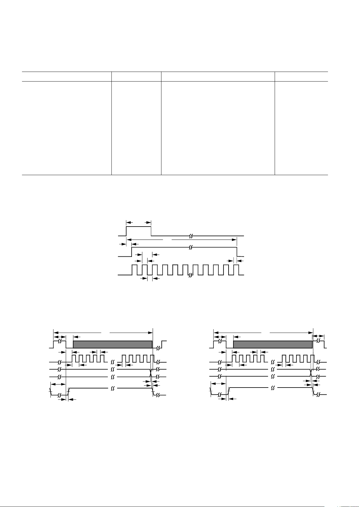
TIMING SPECIFICATIONS
Parameter Symbol Min Typ Max Units
Conversion Time
2
t
C
10 1000 µs
CLK Period
3
t
CLK
480 ns
Calibration Time t
CT
85,530 t
CLK
Sampling Time (Included in t
C
)t
S
2 µs
CAL to BUSY Delay t
CALB
75 150 ns
BUSY to SAMPLE Delay t
BS
2 µs
SAMPLE to BUSY Delay t
SB
15 100 ns
CLK HIGH
4
t
CH
50 ns
CLK LOW
4
t
CL
50 ns
SAMPLE LOW to 1st CLK Delay t
SC
50 ns
SAMPLE LOW t
SL
100 ns
Output Delay t
OD
125 200 ns
Status Delay t
SD
50 ns
CAL HIGH Time t
CALH
50 ns
NOTES
1
See the “CONVERSION CONTROL” and “AUTOCALIBRATION” sections for detailed explanations of the above timing.
2
Depends upon external clock frequency; includes acquisition time and conversion time. The maximum conversion time is specified to account for the droop of the
internal sample/hold function. Longer conversion times may degrade performance. See “General Conversion Guidelines” for additional explanation of maximum con-
version time.
3
580 ns is recommended for optimal accuracy over temperature.
4
t
CH
+ t
CL
= t
CLK
and must be greater than 480 ns.
CAL
BUSY
CLK
t
CH
t
CL
t
CLK
t
CALB
t
OD
t
CT
CALH
t
Figure 1. Calibration Timing
SAMPLE
(INPUT)
CLK
(INPUT)
BIT 1 – BIT 16
(OUTPUTS)
BUSY
(OUTPUT)
12345
t
S
t
SL
t
SC
t
CLK
t
CL
t
CH
t
OD
t
SD
t
SB
t
BS
t
C
13 14 15
16 17
(PREVIOUS CONVERSION)
(NEW DATA)
Figure 2a. General Conversion Timing
SAMPLE
(INPUT)
CLK
(INPUT)
BIT 1 – BIT 16
(OUTPUTS)
BUSY
(OUTPUT)
12345
t
S
t
SL
t
SC
t
CLK
t
CL
t
CH
t
OD
t
SD
t
SB
t
BS
t
C
13 14 15
16 17
t
S
(PREVIOUS CONVERSION)
(NEW DATA)
Figure 2b. Continuous Conversion Timing
(T
MIN
to T
MAX
V
CC
= +12 V 6 5%, V
EE
= –12 V 6 5%, V
DD
= +5 V 6 10%, V
REF
= 10.0 V)
1

AD676
REV. A
–5–
ORDERING GUIDE
Package
Model Temperature Range
1
S/(N+D) Max INL Package Description Option
2
AD676JD 0°C to +70°C 85 dB Ceramic 28-Pin DIP D-28
AD676KD 0°C to +70°C 87 dB ±1.5 LSB Ceramic 28-Pin DIP D-28
AD676AD –40°C to +85°C 85 dB Ceramic 28-Pin DIP D-28
AD676BD –40°C to +85°C 87 dB ±1.5 LSB Ceramic 28-Pin DIP D-28
NOTES
1
For details on grade and package offerings screened in accordance with MIL-STD-883, refer to the AD676/883 data sheet.
2
D = Ceramic DIP.
ABSOLUTE MAXIMUM RATINGS*
V
CC
to V
EE
. . . . . . . . . . . . . . . . . . . . . . . . . . –0.3 V to +26.4 V
V
DD
to DGND . . . . . . . . . . . . . . . . . . . . . . . . . –0.3 V to +7 V
V
CC
to AGND . . . . . . . . . . . . . . . . . . . . . . . . –0.3 V to +18 V
V
EE
to AGND . . . . . . . . . . . . . . . . . . . . . . . . –18 V to +0.3 V
AGND to DGND . . . . . . . . . . . . . . . . . . . . . . . . . . . . ±0.3 V
Digital Inputs to DGND . . . . . . . . . . . . . . . . . . 0 V to +5.5 V
Analog Inputs, V
REF
to AGND
. . . . . . . . . . . . . . . . . . . . . . . (V
CC
+ 0.3 V) to (V
EE
– 0.3 V)
Soldering . . . . . . . . . . . . . . . . . . . . . . . . . . . . . +300°C, 10 sec
Storage Temperature . . . . . . . . . . . . . . . . . . –65°C to +150°C
*Stresses greater than those listed under “Absolute Maximum Ratings” may cause
permanent damage to the device. This is a stress rating only and functional
operation of the device at these or any other conditions above those indicated in
the operational section of this specification is not implied. Exposure to absolute
maximum rating conditions for extended periods may affect device reliability.
WARNING!
ESD SENSITIVE DEVICE
CAUTION
The AD676 features input protection circuitry consisting of large “distributed” diodes and
polysilicon series resistors to dissipate both high energy discharges (Human Body Model) and fast,
low energy pulses (Charged Device Model). Per Method 3015.2 of MIL-STD-883C, the AD676
has been classified as a Category 1 Device.
Proper ESD precautions are strongly recommended to avoid functional damage or performance
degradation. Charges as high as 4000 volts readily accumulate on the human body and test
equipment, and discharge without detection. Unused devices must be stored in conductive foam
or shunts, and the foam discharged to the destination socket before devices are removed. For further
information on ESD Precaution. Refer to Analog Devices’ ESD Prevention Manual.
 Loading...