


AD669
Analog Devices AD669, AD669SQ, AD669BR, AD669BQ, AD669BN Datasheet
...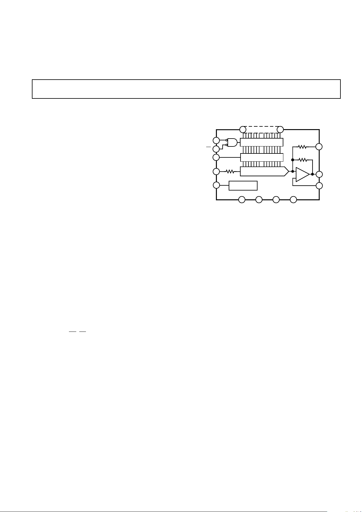
FUNCTIONAL BLOCK DIAGRAM
LDAC
SPAN/
BIP OFF
AGND
DB15
(MSB) (LSB)
DB0
DGND
CS
L1
REF IN
REF OUT
–V
EE
+V
CC
+V
LL
V
OUT
16-BIT LATCH
10k
AMP
AD669
227
6
5
23
27
28
10V REF
2143
26
24
10k
10.05k
16-BIT LATCH
16-BIT DAC
25
REV. A
Information furnished by Analog Devices is believed to be accurate and
reliable. However, no responsibility is assumed by Analog Devices for its
use, nor for any infringements of patents or other rights of third parties
which may result from its use. No license is granted by implication or
otherwise under any patent or patent rights of Analog Devices.
a
Monolithic 16-Bit
DACPORT
AD669
FEATURES
Complete 16-Bit D/A Function
On-Chip Output Amplifier
High Stability Buried Zener Reference
Monolithic BiMOS II Construction
61 LSB Integral Linearity Error
15-Bit Monotonic over Temperature
Microprocessor Compatible
16-Bit Parallel Input
Double-Buffered Latches
Fast 40 ns Write Pulse
Unipolar or Bipolar Output
Low Glitch: 15 nV-s
Low THD+N: 0.009%
MIL-STD-883 Compliant Versions Available
GENERAL DESCRIPTION
The AD669 DACPORT
®
is a complete 16-bit monolithic D/A
converter with an on-board reference and output amplifier. It is
manufactured on Analog Devices’ BiMOS II process. This pro-
cess allows the fabrication of low power CMOS logic functions
on the same chip as high precision bipolar linear circuitry. The
AD669 chip includes current switches, decoding logic, an output
amplifier, a buried Zener reference and double-buffered latches.
The AD669’s architecture insures 15-bit monotonicity over
temperature. Integral nonlinearity is maintained at ± 0.003%,
while differential nonlinearity is ± 0.003% max. The on-chip
output amplifier provides a voltage output settling time of 10 µs
to within 1/2 LSB for a full-scale step.
Data is loaded into the AD669 in a parallel 16-bit format. The
double-buffered latch structure eliminates data skew errors and
provides for simultaneous updating of DACs in a multi-DAC
system. Three TTL/LSTTL/5 V CMOS compatible signals con-
trol the latches:
CS, L1 and LDAC.
The output range of the AD669 is pin programmable and can
be set to provide a unipolar output range of 0 V to +10 V or a
bipolar output range of –10 V to +10 V.
The AD669 is available in seven grades: AN and BN versions
are specified from –40°C to +85°C and are packaged in a 28-pin
plastic DIP. The AR and BR versions are specified for –40°C to
+85°C operation and are packaged in a 28-pin SOIC. The SQ
version is specified from –55°C to +125°C and is packaged in a
hermetic 28-pin cerdip package. The AD669 is also available
compliant to MIL-STD-883. Refer to the AD669/883B data
sheet for specifications and test conditions.
DACPORT is a registered trademark of Analog Devices, Inc.
One Technology Way, P.O. Box 9106, Norwood, MA 02062-9106, U.S.A.
Tel: 617/329-4700 Fax: 617/326-8703
PRODUCT HIGHLIGHTS
1. The AD669 is a complete voltage output 16-bit DAC with
voltage reference and digital latches on a single IC chip.
2. The internal buried Zener reference is laser trimmed to
10.000 volts with a ±0.2% maximum error. The reference
voltage is also available for external applications.
3. The AD669 is both dc and ac specified. DC specs include
±1 LSB INL error and ±1 LSB DNL error. AC specs include
0.009% THD+ N and 83 dB SNR. The ac specifications
make the AD669 suitable for signal generation applications.
4. The double-buffered latches on the AD669 eliminate data
skew errors while allowing simultaneous updating of DACs in
multi-DAC systems.
5. The output range is a pin-programmable unipolar 0 V to
+10 V or bipolar –10 V to +10 V output. No external compo-
nents are necessary to set the desired output range.
6. The AD669 is available in versions compliant with MIL-
STD-883. Refer to the Analog Devices Military Products
Databook or current AD669/883B data sheet for detailed
specifications.

AD669–SPECIFICATIONS
Model AD669AN/AR AD669AQ/SQ AD669BN/BQ/BR
Min Typ Max Min Typ Max Min Typ Max Units
RESOLUTION 16 16 16 Bits
DIGITAL INPUTS (T
MIN
to T
MAX
)
V
IH
(Logic “1” ) 2.0 5.5 * * * * Volts
V
IL
(Logic “0” ) 0 0.8 * * * * Volts
I
IH
(V
IH
= 5.5 V) 610 **µA
I
IL
(V
IL
= 0 V) 610 **µA
TRANSFER FUNCTION CHARACTERISTICS
1
Integral Nonlinearity 62 * 61 LSB
T
MIN
to T
MAX
64 * 62 LSB
Differential Nonlinearity 62 * 61 LSB
T
MIN
to T
MAX
64 * 62 LSB
Monotonicity Over Temperature 14 14 15 Bits
Gain Error
2, 5
60.15 60.10 60.10 % of FSR
Gain Drift
2
(T
MIN
to T
MAX
) 25 15 15 ppm/°C
Unipolar Offset 65 65 62.5 mV
Unipolar Offset Drift (T
MIN
to T
MAX
) 533ppm/°C
Bipolar Zero Error 615 615 610 mV
Bipolar Zero Error Drift (T
MIN
to T
MAX
) 12 10 5 ppm/°C
REFERENCE INPUT
Input Resistance 7 10 13 ****** kΩ
Bipolar Offset Input Resistance 7 10 13 ****** kΩ
REFERENCE OUTPUT
Voltage 9.98 10.00 10.02 ****** Volts
Drift 25 15 15 ppm/°C
External Current
3
24 ** ** mA
Capacitive Load 1000 * * pF
Short Circuit Current 25 * * mA
OUTPUT CHARACTERISTICS
Output Voltage Range
Unipolar Configuration 0 +10 * * * * Volts
Bipolar Configuration –10 +10 * * * * Volts
Output Current 5 * * mA
Capacitive Load 1000 * * pF
Short Circuit Current 25 * * mA
POWER SUPPLIES
Voltage
V
CC
4
+13.5 +16.5 * * * * Volts
V
EE
4
–13.5 –16.5 * * * * Volts
V
LL
+4.5 +5.5 * * * * Volts
Current (No Load)
I
CC
+12 +18 ** ** mA
I
EE
–12 –18 ** ** mA
I
LL
@ V
IH
, V
IL
= 5, 0 V 0.3 2 ** ** mA
@ V
IH
, V
IL
= 2.4, 0.4 V 3 7.5 ** ** mA
Power Supply Sensitivity 1 3 * * * * ppm/%
Power Dissipation (Static, No Load) 365 625 * * mW
TEMPERATURE RANGE
Specified Performance (A, B) –40 +85 –40 +85 –40 +85 °C
Specified Performance (S) –55 +125 °C
NOTES
1
For 16-bit resolution, 1 LSB = 0.0015% of FSR = 15 ppm of FSR. For 15-bit resolution, 1 LSB = 0.003% of FSR = 30 ppm of FSR. For 14-bit resolution
1 LSB = 0.006% of FSR = 60 ppm of FSR. FSR stands for Full-Scale Range and is 10 V for a 0 V to + 10 V span and 20 V for a –10 V to +10 V span.
2
Gain error and gain drift measured using the internal reference. Gain drift is primarily reference related. See the Using the AD669 with the AD688 Reference section
for further information.
3
External current is defined as the current available in addition to that supplied to REF IN and SPAN/BIPOLAR OFFSET on the AD669.
4
Operation on ±12 V supplies is possible using an external reference like the AD586 and reducing the output range. Refer to the Internal/External Reference Use section.
5
Measured with fixed 50 Ω resistors. Eliminating these resistors increases the gain error by 0.25% of FSR (Unipolar mode) or 0.50% of FSR (Bipolar mode). Refer to
the Analog Circuit Connections section.
*Same as AD669AN/AR specification.
Specifications subject to change without notice.
Specifications in boldface are tested on all production units at final electrical test. Results from those tests are used to calculate outgoing quality levels. All min and max specifica-
tions are guaranteed. Those shown in boldface are tested on all production units.
(@ T
A
= +258C,
V
CC
= +15 V, V
EE
= –15 V, V
LL
= +5 V,
unless otherwise noted)
REV. A
–2–
AD669
REV. A
–3–
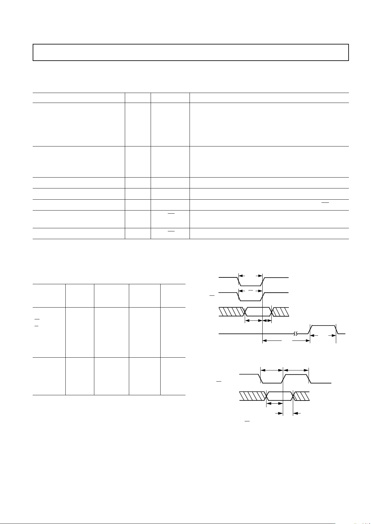
TIMING CHARACTERISTICS
V
CC
= +15 V, V
EE
= –15 V, V
LL
= +5 V, V
HI
= 2.4 V, V
LO
= 0.4 V
Limit Limit
Limit –408C to –558C to
Parameter +258C +858C +1258C Units
(Figure la)
t
CS
40 50 55 ns min
t
LI
40 50 55 ns min
t
DS
30 35 40 ns min
t
DH
10 10 15 ns min
t
LH
90 110 120 ns min
t
LW
40 45 45 ns min
(Figure lb)
t
LOW
130 150 165 ns min
t
HIGH
40 45 45 ns min
t
DS
120 140 150 ns min
t
DH
10 10 15 ns min
Specifications subject to change without notice.
Specifications in boldface are tested on all production units at final electrical
test. Results from those tests are used to calculate outgoing quality levels. All
min and max specifications are guaranteed. Those shown in boldface are tested
on all production units.
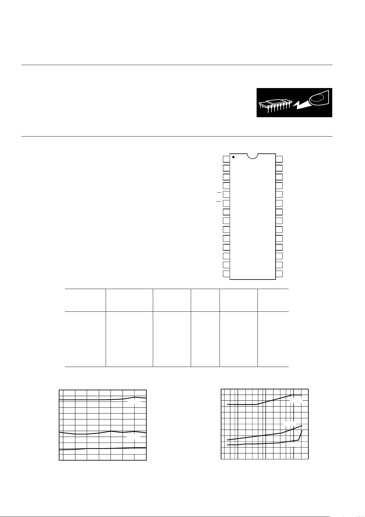
AC PERFORMANCE CHARACTERISTICS
Parameter Limit Units Test Conditions/Comments
Output Settling Time 13 µs max 20 V Step, T
A
= +25°C
(Time to ±0.0008% FS 8 µs typ 20 V Step, T
A
= +25°C
with 2 kΩ, 1000 pF Load) 10 µs typ 20 V Step, T
MIN
≤ T
A
≤ T
MAX
6 µs typ 10 V Step, T
A
= +25°C
8 µs typ 10 V Step, T
MIN
≤ T
A
≤ T
MAX
2.5 µs typ 1 LSB Step, T
MIN
≤ T
A
≤ T
MAX
Total Harmonic Distortion + Noise
A, B, S Grade 0.009 % max 0 dB, 1001 Hz; Sample Rate = 100 kHz; T
A
= +25°C
A, B, S Grade 0.07 % max –20 dB, 1001 Hz; Sample Rate = 100 kHz; T
A
= +25°C
A, B, S Grade 7.0 % max –60 dB, 1001 Hz; Sample Rate = 100 kHz; T
A
= +25°C
Signal-to-Noise Ratio 83 dB min T
A
= +25°C
Digital-to-Analog Glitch Impulse 15 nV-s typ DAC Alternately Loaded with 8000H and 7FFFH
Digital Feedthrough 2 nV-s typ DAC Alternately Loaded with 0000H and FFFFH; CS High
Output Noise Voltage 120 nV/√
Hz typ Measured at V
OUT
, 20 V Span; Excludes Reference
Density (1 kHz – 1 MHz)
Reference Noise 125 nV/√Hz typ Measured at REF OUT
Specifications subject to change without notice.
Specifications in boldface are tested on all production units at final electrical test. Results from those tests are used to calculate outgoing quality levels. All min and
max specifications are guaranteed. Those shown in boldface are tested on all production units.
(With the exception of Total Harmonic Distortion + Noise and Signal-to-Noise
Ratio, these characteristics are included for design guidance only and are not subject to test. THD+N and SNR are 100% tested.
T
MIN
≤ T
A
≤ T
MAX
, V
CC
= +15 V, V
EE
= –15 V, V
LL
= +5 V except where noted.)
DATA
LDAC
t
DS
t
DH
CS
t
LW
t
LH
L1
t
CS
t
L1
Figure 1a. AD669 Level Triggered Timing Diagram
DATA
t
DS
t
DH
CS AND/OR
L1, LDAC
TIE CS AND/OR
L1 TO GROUND OR TOGETHER WITH LDAC
t
LOW
t
HIGH
Figure 1b. AD669 Edge Triggered Timing Diagram
AD669
REV. A
–4–
ORDERING GUIDE
Linearity Gain
Temperature Error Max TC max Package Package
Model Range T
MIN
–T
MAX
ppm/8C Description Option*
AD669AN –40°C to +85°C ±4 LSB 25 Plastic DIP N-28
AD669AR –40°C to +85°C ±4 LSB 25 SOIC R-28
AD669BN –40°C to +85°C ±2 LSB 15 Plastic DIP N-28
AD669BR –40°C to +85°C ±2 LSB 15 SOIC R-28
AD669AQ –40°C to +85°C ±4 LSB 15 Cerdip Q-28
AD669BQ –40°C to +85°C ±2 LSB 15 Cerdip Q-28
AD669SQ –55°C to +125°C ±4 LSB 15 Cerdip Q-28
AD669/883B** –55°C to +125°C** ** ** **
**N = Plastic DIP; Q = Cerdip; R = SOIC.
**Refer to AD669/883B military data sheet.
ESD SENSITIVITY
The AD669 features input protection circuitry consisting of large transistors and polysilicon series
resistors to dissipate both high-energy discharges (Human Body Model) and fast, low-energy pulses
(Charged Device Model). Per Method 3015.2 of MIL-STD-883: C, the AD669 has been classified
as a Class 2 device.
Proper ESD precautions are strongly recommended to avoid functional damage or performance
degradation. Charges as high as 4000 volts readily accumulate on the human body and test
equipment and discharge without detection. Unused devices must be stored in conductive foam or
shunts, and the foam should be discharged to the destination socket before devices are removed.
For further information on ESD precautions, refer to Analog Devices’ ESD Prevention Manual.
WARNING!
ESD SENSITIVE DEVICE
ABSOLUTE MAXIMUM RATINGS
*
V
CC
to AGND . . . . . . . . . . . . . . . . . . . . . . . –0.3 V to +17.0 V
V
EE
to AGND . . . . . . . . . . . . . . . . . . . . . . . +0.3 V to –17.0 V
V
LL
to DGND . . . . . . . . . . . . . . . . . . . . . . . . . . –0.3 V to +7 V
AGND to DGND . . . . . . . . . . . . . . . . . . . . . . . . . . . . . . ±1 V
Digital Inputs (Pins 5 through 23) to DGND . . . . . . –1.0 V to
. . . . . . . . . . . . . . . . . . . . . . . . . . . . . . . . . . . . . . . . . . . . +7.0 V
REF IN to AGND . . . . . . . . . . . . . . . . . . . . . . . . . . . . ±10.5 V
Span/Bipolar Offset to AGND . . . . . . . . . . . . . . . . . . . ±10.5 V
REF OUT, V
OUT
. . . . . . Indefinite Short To AGND, DGND,
. . . . . . . . . . . . . . . . . . . . . . . . . . . . . . . . . . . V
CC
, V
EE
, and V
LL
Power Dissipation (Any Package)
To +60°C . . . . . . . . . . . . . . . . . . . . . . . . . . . . . . . .1000 mW
Derates above +60°C . . . . . . . . . . . . . . . . . . . . . .8.7 mW/°C
Storage Temperature . . . . . . . . . . . . . . . . . . . –65°C to +150°C
Lead Temperature (Soldering, 10 sec) . . . . . . . . . . . . . +300°C
*Stresses above those listed under “Absolute Maximum Ratings” may cause
permanent damage to the device. This is a stress rating only, and functional
operation of the device at these or any other conditions above those indicated in
the operational section of this specification is not implied. Exposure to absolute
maximum rating conditions for extended periods may affect device reliability.
PIN CONFIGURATION
DB15
DB14
DB13
DB12
DB11
DB10
DB9
DB8
DGND
V
EE
V
CC
V
LL
CS
L1
1
2
3
4
5
6
7
8
9
10
11
12
13
14
28
27
26
25
24
23
22
21
20
19
18
17
16
15
TOP VIEW
(Not to Scale)
DB7
DB6
DB5
DB4
DB3
DB2
AGND
LDAC
DB0
DB1
AD669
REF OUT
REF IN
V
OUT
SPAN/BIP
OFFSET
THD + N – %
TEMPERATURE – °C
10
0.001
125
0.01
–25
–50
0.1
1
10075
50250
–60dB
–20dB
0dB
THD+N vs. Temperature
FREQUENCY – Hz
THD + N – %
10
0.001
0.01
0.1
1
100 100001000
–60dB
–20dB
0dB
THD+N vs. Frequency
 Loading...