


AD679TJ
Table of contents
 Loading...
Analog Devices AD679TJ, AD679TD, AD679SJ, AD679SD, AD679KN Datasheet
...
14-Bit 128 kSPS
a
FEATURES
AC and DC Characterized and Specified
(K, B, T Grades)
128k Conversions per Second
1 MHz Full Power Bandwidth
500 kHz Full Linear Bandwidth
80 dB S/N+D (K, B, T Grades)
Twos Complement Data Format (Bipolar Mode)
Straight Binary Data Format (Unipolar Mode)
10 MV Input Impedance
8-Bit Bus Interface (See AD779 for 16-Bit Interface)
On-Board Reference and Clock
10 V Unipolar or Bipolar Input Range
Pin Compatible with AD678 12-Bit, 200 kSPS ADC
MIL-STD-883 Compliant Versions Available
GENERAL DESCRIPTION
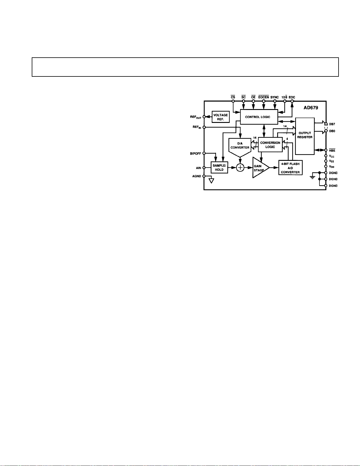
The AD679 is a complete, multipurpose 14-bit monolithic
analog-to-digital converter, consisting of a sample-hold amplifier (SHA), a microprocessor compatible bus interface, a voltage
reference and clock generation circuitry.
The AD679 is specified for ac (or “dynamic”) parameters such
as S/N+D ratio, THD and IMD which are important in signal
processing applications. In addition, the AD679K, B and T
grades are fully specified for dc parameters which are important
in measurement applications.
The 14 data bits are accessed in two read operations (8+6), with
left justification. Data format is straight binary for unipolar
mode and twos complement binary for bipolar mode. The input
has a full-scale range of 10 V with a full power bandwidth of
1 MHz and a full linear bandwidth of 500 kHz. High input impedance (10 MΩ) allows direct connection to unbuffered
sources without signal degradation. Conversions can be initiated
either under microprocessor control or by an external clock
asynchronous to the system clock.
This product is fabricated on Analog Devices’ BiMOS process,
combining low power CMOS logic with high precision, low
noise bipolar circuits; laser-trimmed thin-film resistors provide
high accuracy. The converter utilizes a recursive subranging algorithm which includes error correction and flash converter circuitry to achieve high speed and resolution.
The AD679 operates from +5 V and ±12 V supplies and dissipates 560 mW (typ). 28-pin plastic DIP, ceramic DIP and 44
J-leaded ceramic surface mount packages are available.
*Protected by U.S. Patent Nos. 4,804,960; 4,814,767; 4,833,345; 4,250,445;
4,808,908; RE 30,586
Complete Sampling ADC
AD679*
FUNCTIONAL BLOCK DIAGRAM
PRODUCT HIGHLIGHTS
1. COMPLETE INTEGRATION: The AD679 minimizes
external component requirements by combining a high
speed sample-hold amplifier (SHA), ADC, 5 V reference,
clock and digital interface on a single chip. This provides a
fully specified sampling A/D function unattainable with
discrete designs.
2. SPECIFICATIONS: The AD679K, B and T grades provide
fully specified and tested ac and dc parameters. The AD679J,
A and S grades are specified and tested for ac parameters; dc
accuracy specifications are shown as typicals. DC specifications (such as INL, gain and offset) are important in control
and measurement applications. AC specifications (such as
S/N+D ratio, THD and IMD) are of value in signal processing applications.
3. EASE OF USE: The pinout is designed for easy board layout, and the two read output provides compatibility with 8bit buses. Factory trimming eliminates the need for calibration
modes or external trimming to achieve rated performance.
4. RELIABILITY: The AD679 utilizes Analog Devices’ monolithic BiMOS technology. This ensures long term reliability
compared to multichip and hybrid designs.
5. UPGRADE PATH: The AD679 provides the same pinout as
the 12-bit, 200 kSPS AD678 ADC.
6. The AD679 is available in versions compliant with MILSTD-883. Refer to the Analog Devices Military Products
Databook or current AD679/883B data sheet for detailed
specifications.
REV. C
Information furnished by Analog Devices is believed to be accurate and
reliable. However, no responsibility is assumed by Analog Devices for its
use, nor for any infringements of patents or other rights of third parties
which may result from its use. No license is granted by implication or
otherwise under any patent or patent rights of Analog Devices.
One Technology Way, P.O. Box 9106, Norwood, MA 02062-9106, U.S.A.
Tel: 617/329-4700 Fax: 617/326-8703
AD679–SPECIFICATIONS
(T
to T
, VCC = +12 V 6 5%, VEE = –12 V 6 5%, VDD = +5 V 6 10%, f
MAX
1
AC SPECIFICATIONS
MIN
unless otherwise noted)
AD679J/A/S AD679K/B/T
Parameter Min Typ Max Min Typ Max Units
SIGNAL-TO-NOISE AND DISTORTION (S/N+D) RATIO
2
–0.5 dB Input (Referred to –0 dB Input) 78 79 80 81 dB
–20 dB Input (Referred to –20 dB Input) 58 59 60 61 dB
–60 dB Input (Referred to –60 dB Input) 18 19 20 21 dB
TOTAL HARMONIC DISTORTION (THD)
3
@ +25°C –90 –84 –90 –84 dB
0.003 0.006 0.003 0.006 %
T
MIN
to T
MAX
–88 –82 –88 –82 dB
0.004 0.008 0.004 0.008 %
PEAK SPURIOUS OR PEAK HARMONIC COMPONENT –90 –84 –90 –84 dB
FULL POWER BANDWIDTH 1 1 MHz
FULL LINEAR BANDWIDTH 500 500 kHz
INTERMODULATION DISTORTION (IMD)
4
2nd Order Products –90 –84 –90 –84 dB
3rd Order Products –90 –84 –90 –84 dB
= 128 kSPS, fIN = 10.009 kHz
SAMPLE
DIGITAL SPECIFICATIONS
(All device types T
MIN
to T
, VCC = +12 V 6 5%, VEE = –12 V 6 5%, VDD = +5 V 6 10%)
MAX
Parameter Test Conditions Min Max Units
LOGIC INPUTS
V
IH
V
IL
I
IH
I
IL
C
IN
High Level Input Voltage 2.0 V
DD
V
Low Level Input Voltage 0 0.8 V
High Level Input Current V
Low Level Input Current V
= 5 V –10 +10 µA
IN
= 0 V –10 +10 µA
IN
Input Capacitance 10 pF
LOGIC OUTPUTS
V
OH
V
OL
I
OZ
C
OZ
NOTES
1
flN amplitude = –0.5 dB (9.44 V p-p) bipolar mode full scale unless otherwise indicated. All measurements referred to a –0 dB (9.997 V p-p) input signal
unless otherwise noted.
2
See Figure 15 for higher frequencies and other input amplitudes.
3
See Figures 13 and 14 for higher frequencies and other input amplitudes.
4
fA = 9.08 kHz, fB = 9.58 kHz, with f
Specifications subject to change without notice.
High Level Output Voltage IOH = 0.1 mA 4.0 V
I
= 0.5 mA 2.4 V
OH
Low Level Output Voltage IOL = 1.6 mA 0.4 V
High Z Leakage Current V
= 0 or 5 V –10 +10 µA
IN
High Z Output Capacitance 10 pF
100 kSPS. See Definition of Specifications section.
SAMPLE
REV. C–2–

AD679
(T
to T
DC SPECIFICATIONS
MIN
Parameter Min Typ Max Min Typ Max Units
TEMPERATURE RANGE
J, K Grades 0 +70 0 +70 ° C
A, B Grades –40 +85 –40 +85 °C
S, T Grades –55 +125 –55 +125 °C
ACCURACY
Resolution 14 14 Bits
Integral Nonlinearity (INL) ±2 ±1 62 LSB
Differential Nonlinearity (DNL) 14 14 Bits
Unipolar Zero Error
Bipolar Zero Error
Gain Error
1, 2
Temperature Drift
Unipolar Zero
1
(@ +25°C) 0.08 0.05 0.07 % FSR*
1
(@ +25°C) 0.08 0.05 0.07 % FSR
(@ +25°C) 0.12 0.09 0.11 % FSR
3
J, K Grades 0.04 0.04 0.05 % FSR
A, B Grades 0.05 0.05 0.07 % FSR
S, T Grades 0.09 0.09 0.10 % FSR
Bipolar Zero
3
J, K Grades 0.02 0.02 0.04 % FSR
A, B Grades 0.04 0.04 0.05 % FSR
S, T Grades 0.08 0.08 0.09 % FSR
3
Gain
J, K Grades 0.09 0.09 0.11 % FSR
A, B Grades 0.10 0.10 0.16 % FSR
S, T Grades 0.20 0.20 0.25 % FSR
4
Gain
J, K Grades 0.04 0.04 0.05 % FSR
A, B Grades 0.05 0.05 0.07 % FSR
S, T Grades 0.09 0.09 0.10 % FSR
ANALOG INPUT
Input Ranges
Unipolar Mode 0 +10 0 +10 V
Bipolar Mode –5 +5 –5 +5 V
Input Resistance 10 10 MΩ
Input Capacitance 10 10 pF
Input Settling Time 1.5 1.5 µs
Aperture Delay 10 10 ns
Aperture Jitter 150 150 ps
INTERNAL VOLTAGE REFERENCE
Output Voltage
5
External Load
Unipolar Mode +1.5 +1.5 mA
Bipolar Mode +0.5 +0.5 mA
POWER SUPPLIES
Power Supply Rejection
= +12 V ± 5% ±6 66 LSB
V
CC
= –12 V ± 5% ±6 66 LSB
V
EE
= +5 V ± 10% ±6 66 LSB
V
DD
Operating Current
I
CC
I
EE
I
DD
Power Consumption 560 745 560 745 m
NOTES
1
Adjustable to zero. See Figures 5 and 6.
2
Includes internal voltage reference error.
3
Includes internal voltage reference drift.
4
Excludes internal voltage reference drift.
5
With maximum external load applied.
*% FSR = percent of full-scale range.
Specifications shown in boldface are tested on all devices at final electrical test with worst case supply voltages at T
calculate outgoing quality levels. All min and max specifications are guaranteed, although only those shown in boldface are tested.
Specifications subject to change without notice.
, VCC = +12 V 6 5%, VEE = –12 V 6 5%, VDD = +5 V 6 10% unless otherwise noted)
MAX
AD679J/A/S AD679K/B/T
4.98 5.02 4.98 5.02 V
18 20 18 20 mA
25 34 25 34 mA
8 12 8 12 mA
25°C and T
MIN,
. Results from those tests are used to
MAX
W
REV. C
–3–
AD679
TIMING SPECIFICATIONS
(All device types T
VDD = +5 V 6 10%)
Parameter Symbol Min Max Units
MIN
to T
, VCC = +12 V 6 5%, VEE = –12 V 6 5%,
MAX
SC Delay t
Conversion Time t
Conversion Rate
1
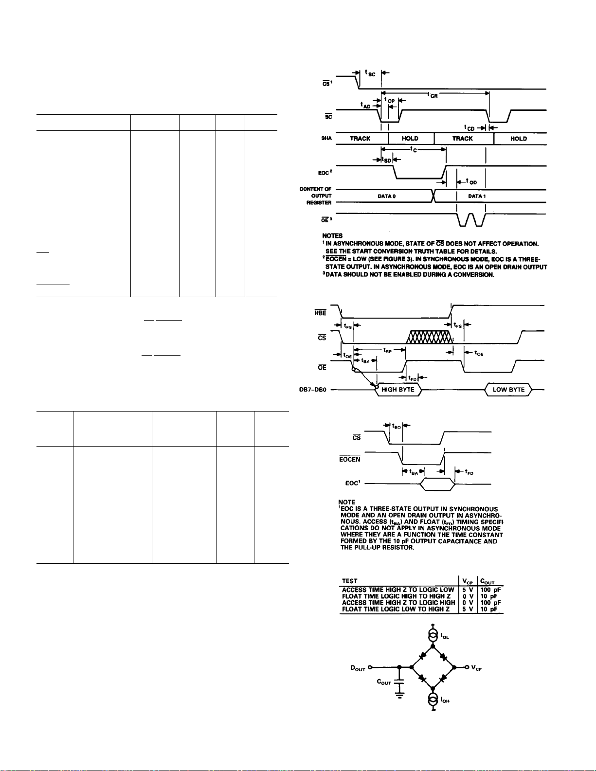
Convert Pulse Width t
Aperture Delay t
Status Delay t
Access Time
Float Delay
2, 3
5
Output Delay t
Format Setup t
OE Delay t
Read Pulse Width t
Conversion Delay t
EOCEN Delay t
NOTES
1
Includes Acquisition Time.
2
Measured from the falling edge of OE/EOCEN (0.8 V) to the time at which the
data lines/EOC cross 2.0 V or 0.8 V. See Figure 4.
3
C
= 100 pF.
OUT
4
C
= 50 pF.
OUT
5
Measured from the rising edge of OE/EOCEN (2.0 V) to the time at which the
output voltage changes by 0.5. See Figure 4; C
Specifications subject to change without notice.
SC
C
t
CR
CP
AD
SD
t
BA
t
FD
OD
FS
OE
RP
CD
EO
ORDERING GUIDE
Model2Package Range Specified Option
Temperature and Package
50 ns
6.3 µs
7.8 µs
0.097 3.0 µs
520ns
0 400 ns
10 100 ns
10 57
4
ns
10 80 ns
0ns
100 ns
20 ns
195 ns
400 ns
50 ns
= 10 pF.
OUT
1
Tested
Figure 1. Conversion Timing
Figure 2. Output Timing
3
AD679JN 28-Pin Plastic DIP 0°C to +70°C AC N-28
AD679KN 28-Pin Plastic DIP 0°C to +70°C AC + DC N-28
AD679JD 28-Pin Ceramic DIP 0°C to +70°C AC D-28
AD679KD 28-Pin Ceramic DIP 0°C to +70°C AC + DC D-28
AD679AD 28-Pin Ceramic DIP –40°C to +85°C AC D-28
AD679BD 28-Pin Ceramic DIP –40°C to +85°C AC + DC D-28
AD679SD 28-Pin Ceramic DIP –55°C to +125°C AC D-28
AD679TD 28-Pin Ceramic DIP –55°C to +125°C AC + DC D-28
AD679AJ 44-Lead Ceramic JLCC –40°C to +85°C AC J-44
AD679BJ 44-Lead Ceramic JLCC –40°C to +85°C AC + DC J-44
AD679SJ 44-Lead Ceramic JLCC –55°C to +125°C AC J-44
AD679TJ 44-Lead Ceramic JLCC –55°C to +125°C AC + DC J-44
NOTES
1
For parallel read (14-bits) interface to 16-bit buses, see AD779.
2
For details grade and package offerings screened in accordance with MIL-STD883, refer to the Analog Devices Miliary Products Databook or current AD679/
883B data sheet.
3
N = Plastic DIP; D = Ceramic DIP; J = J-Leaded Ceramic Chip Carrier.
Figure 3. EOC Timing
Figure 4. Load Circuit for Bus Timing Specifications
REV. C–4–
Loading...