


AD694
Table of contents
 Loading...
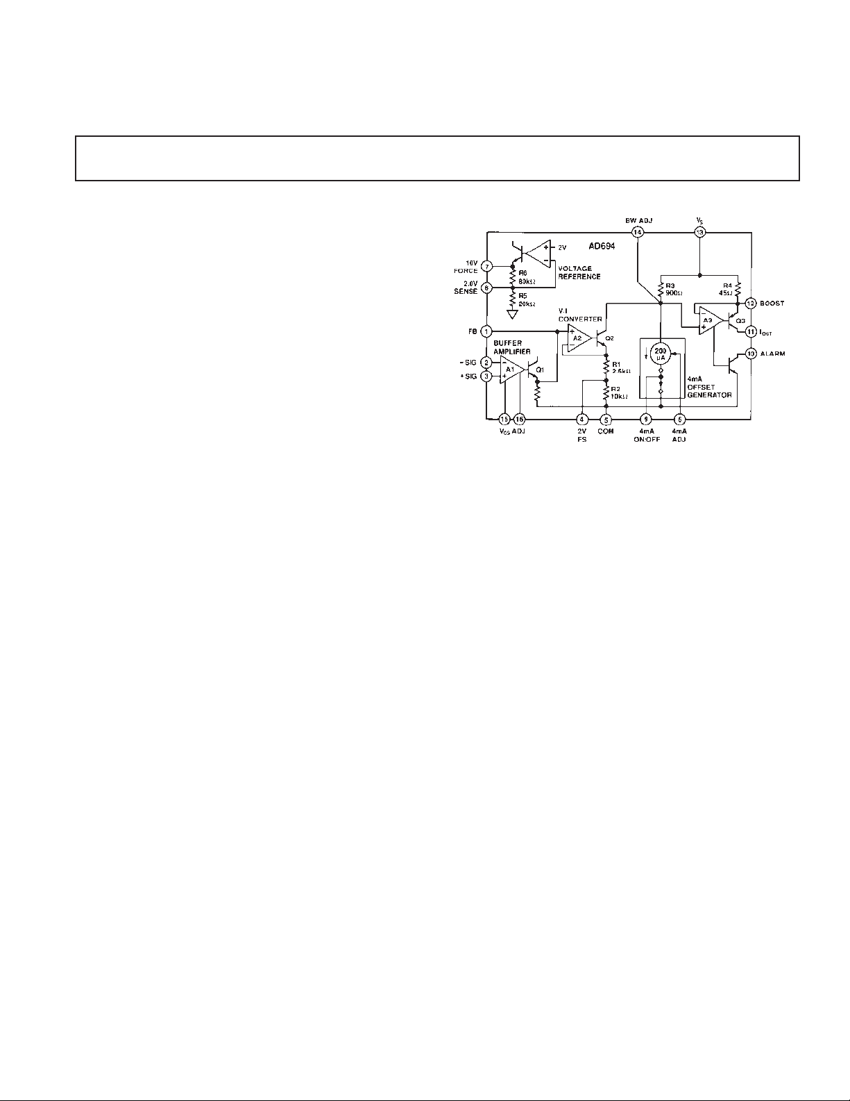
FUNCTIONAL BLOCK DIAGRAM
REV. B
Information furnished by Analog Devices is believed to be accurate and
reliable. However, no responsibility is assumed by Analog Devices for its
use, nor for any infringements of patents or other rights of third parties that
may result from its use. No license is granted by implication or otherwise
under any patent or patent rights of Analog Devices.
a
4–20 mA Transmitter
AD694*
FEATURES
4–20 mA, 0–20 mA Output Ranges
Precalibrated Input Ranges:
0 V to 2 V, 0 V to 10 V
Precision Voltage Reference
Programmable to 2.000 V or 10.000 V
Single or Dual Supply Operation
Wide Power Supply Range: 4.5 V to 36 V
Wide Output Compliance
Input Buffer Amplifier
Open-Loop Alarm
Optional External Pass Transistor to Reduce
Self-Heating Errors
0.002% Typ Nonlinearity
PRODUCT DESCRIPTION
The AD694 is a monolithic current transmitter that accepts
high level signal inputs to drive a standard 4–20 mA current
loop for the control of valves, actuators, and other devices com-
monly used in process control. The input signal is buffered by
an input amplifier that can be used to scale the input signal or
buffer the output from a current mode DAC. Precalibrated in-
put spans of 0 V to 2 V and 0 V to 10 V are selected by simple
pin strapping; other spans may be programmed with external
resistors.
The output stage compliance extends to within 2 V of V
S
and
its special design allows the output voltage to extend below
common in dual supply operation. An alarm warns of an open
4–20 mA loop or noncompliance of the output stage.
Active laser trimming of the AD694’s thin film resistors results
in high levels of accuracy without the need for additional adjust-
ments and calibration. An external pass transistor may be used
with the AD694 to off-load power dissipation, extending the
temperature range of operation.
The AD694 is the ideal building block for systems requiring
noise immune 4–20 mA signal transmission to operate valves,
actuators, and other control devices, as well as for the transmis-
sion of process parameters such as pressure, temperature, or
flow. It is recommended as a replacement for discrete designs in
a variety of applications in industrial process control, factory
automation, and system monitoring.
The AD694 is available in hermetically sealed, 16-pin CERDIP
and plastic SOIC, specified over the –40°C to +85°C industrial
temperature range, and in a 16-pin plastic DIP, specified over
the 0°C to +70°C temperature range.
*Protected by U.S. Patents: 30,586; 4,250,445; 4,857,862.
One Technology Way, P.O. Box 9106, Norwood, MA 02062-9106, U.S.A.
Tel: 781/329-4700 www.analog.com
Fax: 781/326-8703 © Analog Devices, Inc., 2002
PRODUCT HIGHLIGHTS
1. The AD694 is a complete voltage in to 4–20 mA out current
transmitter.
2. Pin programmable input ranges are precalibrated at 0 V to
2 V and 0 V to 10 V.
3. The input amplifier may be configured to buffer and scale the
input voltage, or to serve as an output amplifier for current
output DACs.
4. The output voltage compliance extends to within 2 V of the
positive supply and below common. When operated with a
5 V supply, the output voltage compliance extends 30 V be-
low common.
5. The AD694 interfaces directly to 8-, 10-, and 12-bit single
supply CMOS and bipolar DACs.
6. The 4 mA zero current may be switched on and off with a
TTL control pin, allowing 0–20 mA operation.
7. An open collector alarm warns of loop failure due to open
wires or noncompliance of the output stage.
8. A monitored output is provided to drive an external pass
transistor. The feature off-loads power dissipation to extend
the temperature range of operation and minimize self-heating
error.

AD694–SPECIFICATIONS
Model AD694JN/AQ/AR AD694BQ/BR
Min Typ Max Min Typ Max Unit
INPUT CHARACTERISTICS
Input Voltage Range –0.2 V
S
–2.0 V V
S
–2.5 V –0.2 V
S
–2.0 V V
S
–2.5 V V
Input Bias Current
Either Input, T
MIN
to T
MAX
1.5 5 1.5 5 nA
Offset Current, T
MIN
to T
MAX
± 0.1 ⴞ1 ± 0.1 ⴞ1 nA
Offset Current Drift ± 1.0 ± 5.0 ± 1.0 ± 5.0 pA/°C
Input Impedance 5 5 MΩ
OUTPUT CHARACTERISTICS
Operating Current Range 0 23 0 23 mA
Specified Performance 4 20 4 20 mA
Output Voltage Compliance V
S
–36 V V
S
–2 V V
S
–36 V V
S
2 V V
Output Impedance, 4–20 mA 40.0 50.0 40.0 50.0 MΩ
Current Limit (@ 2 × FS Overdrive 24 44 24 44 mA
Slew Rate 1.3 1.3 mA/µs
SPAN AND ZERO ACCURACY
1
4 mA Offset Error @ 0 V Input
2
Error from 4.000 mA, 4 mA On ± 10 ⴞ20 ± 5 ⴞ10 µA
Error from 0.000 mA, 4 mA Off 0 +10 +20 0+5+10 µA
T
MIN
to T
MAX
± 10 ⴞ40 ± 5 ⴞ20 µA
vs. Supply (2 V Span/10 V Span) 0.3/0.05 0.8/0.4 0.3/0.05 0.8/0.4 µA/V
Trim Range, 4 mA Zero 2.0 4.8 2.0 4.8 mA
Span
Nominal Transfer Function
Input FS = 2 V 8.0 8.0 mA/V
Input FS = 10 V 1.6 1.6 mA/V
Transfer Function Error from Nom,
Input FS = 2 V, 10 V ± 0.1 ⴞ0.3 ± 0.05 ⴞ0.15 % of Span
T
MIN
to T
MAX
± 0.002 ± 0.005 ± 0.001 ⴞ0.0025 % of Span/°C
vs. Supply ± 0.001 ⴞ0.005 ± 0.001 ⴞ0.005 % of Span/V
Nonlinearity
3
± 0.005 ⴞ0.015 ± 0.001 ⴞ0.005 % of Span
4 mA On: Max Pin 9 Voltage 0.8 0.8 V
4 mA Off: Min Pin 9 Voltage 3.0 2.5 3.0 2.5 V
VOLTAGE REFERENCE
Output Voltage: 10 V Reference 9.960 10.000 10.040 9.980 10.000 10.020 V
Output Voltage: 2 V Reference 1.992 2.000 2.008 1.996 2.000 2.004 V
T
MIN
to T
MAX
4
30 50 20 30 ppm/°C
vs. Load, V
REF
= 2 V, 10 V 0.15 0.50 0.15 0.50 mV/mA
vs. Supply, V
REF
= 2 V, 10 V ±0.001 ⴞ0.005 ±0.001 ⴞ0.005 %/V
Output Current
Source 5 5mA
Sink 0.2 0.2 mA
ALARM CHARACTERISTICS
V
CE(SAT)
@ 2.5 mA 0.35 0.35 V
Leakage Current ⴞ1 ⴞ1 µA
Alarm Pin Current (Pin 10) 20 20 mA
POWER REQUIREMENTS
Specified Performance 24 24 V
Operating Range
2 V FS, V
REF
= 2 V 4.5 36 4.5 36 V
2 V, 10 V FS, V
REF
= 2 V, 10 V 12.5 36 12.5 36 V
Quiescent Current, 4 mA Off 1.5 2.0 1.5 2.0 mA
TEMPERATURE RANGE
Specified Performance
5
AD694AQ/BQ/AR/BR –40 +85 –40 +85 °C
AD694JN 0 +70 0 +70 °C
Operating AD694AQ/BQ/AR/BR –55 +125 –55 +125 °C
AD694JN –40 +85 –40 +85 °C
(@ +25ⴗC, R
L
= 250 ⍀, and V
S
= +24 V, unless otherwise noted.)
REV. B
–2–
Model AD694JN/AQ/AR AD694BQ/BR
Min Typ Max Min Typ Max Unit
BUFFER AMPLIFIER
6
Input Offset Voltage
Initial Offset ± 150 ⴞ500 ± 50 ⴞ500 µV
T
MIN
to T
MAX
± 2 ± 3 ± 2 ± 3 µV/°C
vs. Supply 80 90 80 90 dB
vs. Common Mode 80 90 80 90 dB
Trim Range ⴞ2.5 ± 4.0 ⴞ2.5 ± 4.0 mV
Frequency Response
Unity Gain, Small Signal 300 300 kHz
Input Voltage Noise (0.1 Hz to 10 Hz) 2 2 µV p-p
Open-Loop Gain
V
O
= +10 V, R
L
≥ 10 kΩ 50 50 V/mV
Output Voltage @ Pin 1, FB
1
Minimum Output Voltage 1.0 10 1.0 10 mV
Maximum Output Voltage V
S
–2.5 V V
S
–2 V V
S
–2.5 V V
S
–2 V V
NOTES
1
The single supply op amps of the AD694, lacking pull down current, may not reach 0.000 V at their outputs. For this reason, span, offset, and nonlinearity are
specified with the input amplifiers operating in their linear range. The input voltage used for the tests is 5 mV to 2 V and 5 mV to 10 V for the two precalibrated
input ranges. Span and zero accuracy are tested with the buffer amplifier configured as a follower.
2
Offset at 4 mA out and 0 mA out are extrapolated to 0.000 V input from measurements made at 5 mV and at full scale. See Note 1.
3
Nonlinearity is specified as the maximum deviation of the output, as a % of span, from a straight line drawn through the endpoints of the transfer function.
4
Voltage reference drift guaranteed by the Box Method. The voltage reference output over temperature will fall inside of a box whose length is determined by the
temperature range and whose height is determined by the maximum temperature coefficient multiplied by the temperature span in degrees C.
5
Devices tested at these temperatures with a pass transistor. Allowable temperature range of operation is dependent upon internal power dissipation. Absolute
maximum junction and case temperature should not be exceeded. See section: “Power Dissipation Considerations.”
6
Buffer amplifier specs for reference. Buffer amplifier offset and drift already included in Span and Zero accuracy specs above.
Specifications subject to change without notice.
Specifications shown in boldface are tested on all production units at final electrical test. Results from those tests are used to calculate outgoing quality levels.
All min and max specifications are guaranteed, although only those shown in boldface are tested on all production units.
AD694
–3–
REV. B
PIN CONFIGURATION (N, R, Q PACKAGE)
ABSOLUTE MAXIMUM RATINGS
Supply Voltage . . . . . . . . . . . . . . . . . . . . . . . . . . . . . . . . . .36 V
V
S
to I
OUT
. . . . . . . . . . . . . . . . . . . . . . . . . . . . . . . . . . . . .36 V
Input Voltage, (Either Input Pin 2 or 3) . . . . . –0.3 V to +36 V
Reference Short Circuit to Common . . . . . . . . . . . . Indefinite
Alarm Voltage, Pin 10 . . . . . . . . . . . . . . . . . . . . . . . . . . . .36 V
4 mA Adj, Pin 6 . . . . . . . . . . . . . . . . . . . . . . . . . . . . . . . . . .1 V
4 mA On/Off, Pin 9 . . . . . . . . . . . . . . . . . . . . . . . . 0 V to 36 V
Storage Temperature Range
AD694Q . . . . . . . . . . . . . . . . . . . . . . . . . .–65°C to +150°C
AD694N, R . . . . . . . . . . . . . . . . . . . . . . . .–65°C to +125°C
Lead Temperature, 10 sec Soldering . . . . . . . . . . . . . . . 300°C
Maximum Junction Temperature . . . . . . . . . . . . . . . . . 150°C
Maximum Case Temperature
Plastic Package (N, R) . . . . . . . . . . . . . . . . . . . . . . . . 125°C
Cerdip Package (Q) . . . . . . . . . . . . . . . . . . . . . . . . . . 125°C
ORDERING GUIDE
Temperature Package
Model Range Option*
AD694JN 0°C to 70°C N-16
AD694AQ –40°C to +85°CQ-16
AD694AR –40°C to +85°C R-16
AD694BQ –40°C to +85°CQ-16
AD694BR –40°C to +85°C R-16
*N = Plastic DIP; Q = CERDIP, R = SOIC
Transistor Count: . . . . . . . . . . . . . . . . . . . . .75 Active Devices
Substrate Connection: . . . . . . . . . . . . . . . . . . . . to Com, Pin 5
Thermal Characteristics:
Plastic (N) Package: θ
JC
= 50°C/Watt
θ
CA
(Still Air) = 85°C/Watt
Cerdip (Q) Package: θ
JC
= 30°C/Watt
θ
CA
(Still Air) = 70°C/Watt
Plastic (R) Package: θ
JC
= 27°C/Watt
θ
CA
(Still Air) = 73°C/Watt
ESD Susceptibility
All pins are rated for a minimum of 4000 V protection, except
for Pins 2, 3 and 9 which are rated to survive a minimum of
1500 V. ESD testing conforms to Human Body Model. Always
practice ESD prevention.
No pin, other than I
OUT
(11) and ± Sig (2), (3) as noted, may be permitted to become more negative than Com (5). No pin may be
permitted to become more positive than V
S
(13).
AD694
–4–
REV. B
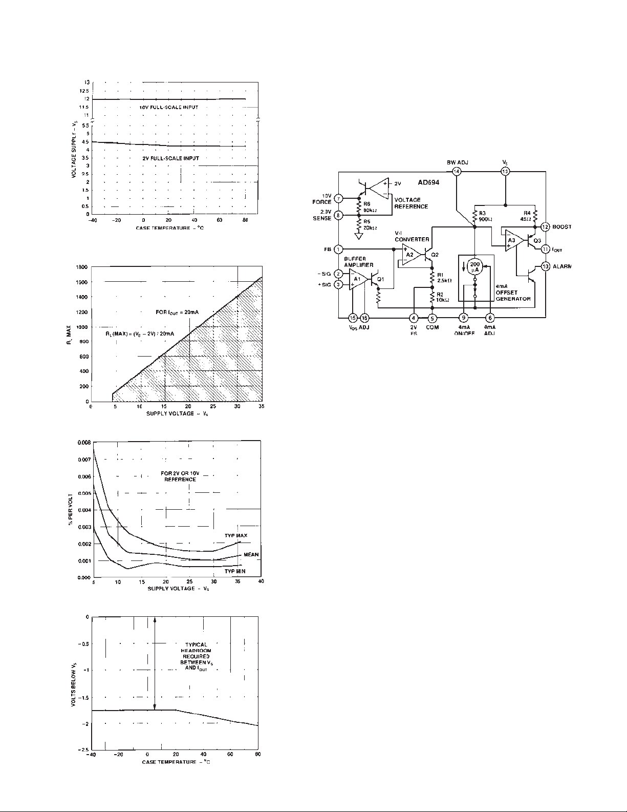
Typical Minimum Supply Voltage vs. Temperature for 2 V
and 10 V Full Scale
Maximum R
L
vs. Supply Voltage
Voltage Reference Power Supply Rejection
I
OUT
: Voltage Compliance vs. Temperature
FUNCTIONAL DESCRIPTION
The operation of the AD694 can best be understood by dividing
the circuit into three functional parts (see Figure 1). First, a
single supply input amplifier buffers the high level, single-ended
input signal. The buffer amplifier drives the second section, a
voltage to current (V/I) converter, that makes a 0 to 16 mA sig-
nal dependent current.
Figure 1. Functional Block Diagram
The third section, a voltage reference and offset generator, is re-
sponsible for providing the 4 mA offset current signal.
BUFFER AMPLIFIER
The buffer amplifier is a single supply amplifier that may be
used as a unity gain buffer, an output amplifier for a current
output DAC, or as a gain block to amplify low level signals. The
amplifier’s PNP input stage has a common-mode range that ex-
tends from a few hundred mV below ground to within 2.5 V of
V
S
. The Class A output of the amplifier appears at Pin 1 (FB).
The output range extends from about 1 mV above common to
within 2.5 V of V
S
when the amplifier is operated as a follower.
The amplifier can source a maximum load of 5 kΩ, but can sink
only as much as its internal 10 kΩ pulldown resistor allows.
V/I CONVERTER
The ground referenced, input signal from the buffer amplifier is
converted to a 0 to 0.8 mA current by A2 and level shifted to
the positive supply. A current mirror then multiplies this signal
by a factor of 20 to make the signal current of 0 to 16 mA. This
technique allows the output stage to drive a load to within 2 V
of the positive supply (V
S
). Amplifier A2 forces the voltage at
Pin 1 across resistors R1 and R2 by driving the Darlington tran-
sistor, Q2. The high gain Darlington transmits the resistor cur-
rent to its collector and to R3 (900 Ω). A3 forces the level
shifted signal across the 45 Ω resistor to get a current gain of 20.
The transfer function of the V/I stage is therefore:
IVR1R2
OUT PIN1
=× +
()
20 /
resulting in a 0-16 mA output swing for a 0–10 V input. Tying
Pin 4 (2 V FS) to ground shorts out R2 and results in a 2 V
full-scale input for a 16 mA output span.
The output stage of the V/I converter is of a unique design that
allows the I
OUT
pin to drive a load below the common (sub-
strate) potential of the device. The output transistor can always
drive a load to a point 36 V below the positive supply (V
S
). An
AD694
REV. B
–5–
Table I. Precalibrated Ranges for the AD694
I
nput Output Voltage Min
Range Range Reference V
S
Pin 9 Pin 4 Pin 8
0–2 V 4–20 mA 2 V 4.5 V Pin 5 Pin 5 Pin 7
0–10 V 4–20 mA 2 V 12.5 V Pin 5 Open Pin 7
0–2.5 V 0–20 mA 2 V 5.0 V ≥3 V Pin 5 Pin 7
0–12.5 V 0–20 mA 2 V 15.0 V ≥3 V Open Pin 7
0–2 V 4–20 mA 10 V 12.5 V Pin 5 Pin 5 Open
0–10 V 4–20 mA 10 V 12.5 V Pin 5 Open Open
0–2.5 V 0–20 mA 10 V 12.5 V ≥3 V Pin 5 Open
0–12.5 V 0–20 mA 10 V 15.0 V ≥3 V Open Open
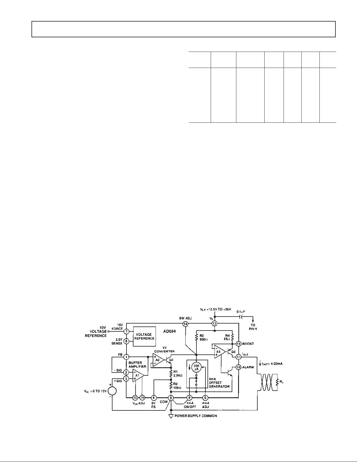
BASIC CONNECTIONS: 12.5 V SINGLE-SUPPLY
OPERATION WITH 10 V FS
Figure 2 shows the minimal connections required for basic
operation with a 12.5 V power supply, 10 V input span,
4–20 mA output span, and a 10 V voltage reference. The buffer
amplifier is connected as a voltage follower to drive the V/I
converter by connecting FB (Pin 1) to –Sig (Pin 2). 4 mA On/
Off (Pin 9) is tied to ground (Pin 5) to enable the 4 mA offset
current. The AD694 can drive a maximum load R
L
= [V
S
– 2 V]
/20 mA, thus the maximum load with a 12.5 V supply is 525 Ω.
SELECTING A 2 V FULL-SCALE INPUT
The 2 V full-scale option is selected by shorting Pin 4 (2 V FS)
to Pin 5 (Common). The connection should be as short as pos-
sible; any parasitic resistance will affect the precalibrated span
accuracy.
SELECTING THE 2 V VOLTAGE REFERENCE
The voltage reference is set to a 2 V output by shorting Pin 7 to
Pin 8 (10 V Force to 2 V Sense). If desired, the 2 V reference
can be set up for remote force and sense connection. Keep in
mind that the 2 V Sense line carries a constant current of 100 µA
that could cause an offset error over long wire runs. The 2 V
reference option can be used with all supply voltages greater
than 4.5 V.
optional NPN pass transistor can be added to transfer most of
the power dissipation off-chip, to extend the temperature range
of operation.
The output stage is current-limited at approximately 38 mA to
protect the output from an overdrive at its inputs. The V/I will
allow linear operation to approximately 24 mA. The V/I con-
verter also has an open collector alarm (Pin 10) which warns of
open-circuit condition at the I
OUT
pin or of attempts to drive the
output to a voltage greater than V
S
– 2 V.
4 mA OFFSET GENERATOR
This circuit converts a constant voltage from the voltage
reference to a constant current of approximately 200 µA. This
current is summed with the signal current at Pin 14 (BW
Adjust), to result in a constant 4 mA offset current at I
OUT
. The
4 mA Adj (Pin 6) allows the offset current to be adjusted to any
current in the range of 2 mA to 4.8 mA. Pin 9 (4 mA On/Off)
can shut off the offset current completely if it is lifted to 3.0 V or
more, allowing 0 to 20 mA operation of the AD694. In normal
4–20 mA operation, Pin 9 is connected to ground.
VOLTAGE REFERENCE
A 2 V or 10 V voltage reference is available for user applications,
selectable by pin-strapping. The 10 V option is available for
supply voltages greater than 12.5 V, the 2 V output is available
over the whole 4.5 V to 36 V power supply range. The reference
can source up to 5 mA for user applications. A boost transistor
can be added to increase the current drive capability of the 2 V
mode.
APPLYING THE AD694
The AD694 can easily be connected for either dual or single
supply operation, to operate from supplies as low as 4.5 V and
as high as 36 V. The following sections describe the different
connection configurations, as well as adjustment methods.
Table I shows possible connection options.
Figure 2. Minimal Connections for 0 V to 10 V Single-Ended Input, 4–20 mA Output, 10 V Reference Output
Loading...