


 Loading...
a |
14A/D-Bit,Converter80 MSPS |
|
AD6645 |
|
|
FEATURES
80 MSPS Guaranteed Sample Rate SNR = 75 dB, fIN 15 MHz @ 80 MSPS SNR = 72 dB, fIN 200 MHz @ 80 MSPS
SFDR = 89 dBc, fIN 70 MHz @ 80 MSPS 100 dB Multitone SFDR
IF Sampling to 200 MHz Sampling Jitter 0.1 ps 1.5 W Power Dissipation
Differential Analog Inputs Pin-Compatible to AD6644
Two’s Complement Digital Output Format 3.3 V CMOS-Compatible
DataReady for Output Latching
APPLICATIONS
Multichannel, Multimode Receivers
Base Station Infrastructure
AMPS, IS-136, CDMA, GSM, WCDMA
Single Channel Digital Receivers
Antenna Array Processing
Communications Instrumentation
Radar, Infrared Imaging
Instrumentation
PRODUCT DESCRIPTION
The AD6645 is a high-speed, high-performance, monolithic 14-bit analog-to-digital converter. All necessary functions, including track-and-hold (T/H) and reference, are included on the chip to provide a complete conversion solution. The AD6645 provides CMOS-compatible digital outputs. It is the fourth
generation in a wideband ADC family, preceded by the AD9042 (12-bit, 41 MSPS), the AD6640 (12-bit, 65 MSPS, IF sampling), and the AD6644 (14-bit, 40 MSPS/65 MSPS).
Designed for multichannel, multimode receivers, the AD6645 is part of Analog Device’s SoftCell™ transceiver chipset. The AD6645 maintains 100 dB multitone, spurious-free dynamic range (SFDR) through the second Nyquist band. This breakthrough performance eases the burden placed on multimode digital receivers (software radios) that are typically limited by the ADC. Noise performance is exceptional; typical signal-to- noise ratio is 74.5 dB through the first Nyquist band.
The AD6645 is built on Analog Devices’ high-speed complementary bipolar process (XFCB) and uses an innovative, multipass circuit architecture. Units are available in a thermally enhanced 52lead PowerQuad 4® (LQFP_ED) specified from –40∞C to +85∞C.
PRODUCT HIGHLIGHTS
1.IF Sampling
The AD6645 maintains outstanding ac performance up to input frequencies of 200 MHz. Suitable for multicarrier 3G wideband cellular IF sampling receivers.
2.Pin Compatibility
The ADC has the same footprint and pin layout as the AD6644, 14-Bit 40 MSPS/65 MSPS ADC.
3.SFDR Performance and Oversampling
Multitone SFDR performance of –100 dBc can reduce the requirements of high-end RF components and allows the use of receive signal processors such as the AD6620 or AD6624/ AD6624A.
|
|
|
|
|
FUNCTIONAL BLOCK DIAGRAM |
|
|
|
|
|
|
|
||||||
|
AVCC |
DVCC |
|
|
|
|
|
|
|
|
|
|
|
|
|
|
|
|
|
|
|
|
|
|
|
|
AD6645 |
|
|
|
|
|
|
|
|
|
|
AIN |
A1 |
TH1 |
TH2 |
|
|
|
A2 |
TH3 |
|
|
TH4 |
|
|
|
TH5 |
|
ADC3 |
|
AIN |
|
|
|
|
|
|
|
|
|
|
||||||||
|
|
|
|
|
|
|
|
|
|
|
|
|
|
|
|
|
|
|
VREF |
2.4V |
|
ADC1 |
|
DAC1 |
|
|
|
|
ADC2 |
DAC2 |
|
|
|
|
6 |
||
|
|
|
|
|
|
|
|
|
|
|
|
|
|
|
|
|
||
|
|
|
|
5 |
|
|
|
|
|
|
|
5 |
|
|
|
|
|
|
ENCODE |
INTERNAL |
|
|
|
|
|
DIGITAL ERROR CORRECTION LOGIC |
|
|
|
|
|
|
|||||
|
|
|
|
|
|
|
|
|
|
|
|
|||||||
ENCODE |
TIMING |
|
|
|
|
|
|
|
|
|
|
|
||||||
|
|
|
|
|
|
|
|
|
|
|
|
|
|
|
|
|||
|
|
|
|
|
|
|
|
|
|
|
|
|
|
|
|
|
|
|
|
GND |
DMID |
OVR |
DRY |
D13 |
D12 |
D11 |
D10 |
D9 |
D8 |
D7 |
D6 |
D5 |
D4 |
D3 |
D2 |
D1 |
D0 |
|
|
|
|
|
MSB |
|
|
|
|
|
|
|
|
|
|
|
|
LSB |
SoftCell is a trademark of Analog Devices, Inc.
PowerQuad 4 is a registered trademark of Amkor Technology, Inc.
REV. 0
Information furnished by Analog Devices is believed to be accurate and reliable. However, no responsibility is assumed by Analog Devices for its use, nor for any infringements of patents or other rights of third parties that may result from its use. No license is granted by implication or otherwise under any patent or patent rights of Analog Devices.
One Technology Way, P.O. Box 9106, Norwood, MA 02062-9106, U.S.A.
Tel: 781/329-4700 |
www.analog.com |
Fax: 781/326-8703 |
© Analog Devices, Inc., 2002 |
AD6645–SPECIFICATIONS
DC SPECIFICATIONS (AVCC = 5 V, DVCC = 3.3 V; TMIN = –40 C, TMAX = +85 C, unless otherwise noted.)
|
|
|
|
AD6645ASQ-80 |
|
|
Parameter |
Temp |
Test Level |
Min |
Typ |
Max |
Unit |
|
|
|
|
|
|
|
RESOLUTION |
|
|
|
14 |
|
Bits |
|
|
|
|
|
|
|
ACCURACY |
|
|
|
|
|
|
No Missing Codes |
Full |
II |
|
Guaranteed |
|
|
Offset Error |
Full |
II |
–10 |
+1.2 |
+10 |
mV |
Gain Error |
Full |
II |
–10 |
0 |
+10 |
% FS |
Differential Nonlinearity (DNL) |
Full |
II |
–1.0 |
± 0.25 |
+1.5 |
LSB |
Integral Nonlinearity (INL) |
Full |
V |
|
± 0.5 |
|
LSB |
|
|
|
|
|
|
|
TEMPERATURE DRIFT |
|
|
|
|
|
ppm/∞C |
Offset Error |
Full |
V |
|
1.5 |
|
|
Gain Error |
Full |
V |
|
48 |
|
ppm/∞C |
POWER SUPPLY REJECTION (PSRR) |
25∞C |
V |
|
± 1.0 |
|
mV/V |
|
|
|
|
|
|
|
REFERENCE OUT (VREF)1 |
Full |
V |
|
2.4 |
|
V |
ANALOG INPUTS (AIN, AIN) |
|
|
|
|
|
|
Differential Input Voltage Range |
Full |
V |
|
2.2 |
|
V p-p |
Differential Input Resistance |
Full |
V |
|
1 |
|
kW |
Differential Input Capacitance |
25∞C |
V |
|
1.5 |
|
pF |
POWER SUPPLY |
|
|
|
|
|
|
Supply Voltages |
|
|
|
|
|
|
AVCC |
Full |
II |
4.75 |
5.0 |
5.25 |
V |
DVCC |
Full |
II |
3.0 |
3.3 |
3.6 |
V |
Supply Current |
|
|
|
|
|
|
I AVCC (AVCC = 5.0 V) |
Full |
II |
|
275 |
320 |
mA |
I DVCC (DVCC = 3.3 V) |
Full |
II |
|
32 |
45 |
mA |
Rise Time2 |
|
|
|
|
|
|
AVCC |
Full |
IV |
|
|
TBD |
ms |
POWER CONSUMPTION |
Full |
II |
|
1.5 |
1.75 |
W |
|
|
|
|
|
|
|
NOTES
1VREF is provided for setting the common-mode offset of a differential amplifier such as the AD8138 when a dc-coupled analog input is required. VREF should be buffered if used to drive additional circuit functions.
2Specified for dc supplies with linear rise-time characteristics. The use of dc supplies with linear rise-times of <45 ms is highly recommended.
Specifications subject to change without notice
DIGITAL SPECIFICATIONS (AVCC = 5 V, DVCC = 3.3 V; TMIN = –40 C, TMAX = +85 C, unless otherwise noted.)
|
|
|
|
AD6645ASQ-80 |
|
|
Parameter (Conditions) |
Temp |
Test Level |
Min |
Typ |
Max |
Unit |
|
|
|
|
|
|
|
ENCODE INPUTS (ENC, ENC) |
|
|
|
|
|
|
Differential Input Voltage1 |
Full |
IV |
0.4 |
|
|
V p-p |
Differential Input Resistance |
25∞C |
V |
|
10 |
|
kW |
Differential Input Capacitance |
25∞C |
V |
|
2.5 |
|
pF |
LOGIC OUTPUTS (D13–D0, DRY, OVR2) |
|
|
|
|
|
|
Logic Compatibility |
|
|
|
CMOS |
|
|
Logic “1” Voltage (DVCC = 3.3 V)3 |
Full |
II |
2.85 |
DVCC – 0.2 |
|
V |
Logic “0” Voltage (DVCC = 3.3 V)3 |
Full |
II |
|
0.2 |
0.5 |
V |
Output Coding |
|
|
|
Two’s Complement |
|
|
DMID |
Full |
V |
|
DVCC/2 |
|
V |
NOTES
1All ac specifications tested by driving ENCODE and ENCODE differentially.
2The functionality of the Over-Range bit is specified for a temperature range of 25∞C to 85∞C only.
3Digital output logic levels: DVCC = 3.3 V, CLOAD = 10 pF. Capacitive loads >10 pF will degrade performance.
Specifications subject to change without notice.
–2– |
REV. 0 |
|
|
|
|
|
|
|
|
AD6645 |
|
|
1 |
(AVCC = 5 V, DVCC = 3.3 V; ENCODE and ENCODE = 80 MSPS; TMIN = –40 C, TMAX = +85 C, unless |
|||||||
AC SPECIFICATIONS |
otherwise noted.) |
|
|
|
|
|
|
||
|
|
|
|
|
|
AD6645ASQ-80 |
|
|
|
Parameter (Conditions) |
|
Temp |
Test Level |
Min |
Typ |
Max |
Unit |
||
|
|
|
|
|
|
|
|
|
|
SNR |
|
|
25∞C |
|
|
|
|
|
|
Analog Input |
15.5 MHz |
V |
|
75.0 |
|
dB |
|||
@ –1 dBFS |
30.5 MHz |
25∞C |
II |
72.5 |
74.5 |
|
dB |
||
|
70.0 MHz |
25∞C |
II |
72.0 |
73.5 |
|
dB |
||
|
150.0 MHz |
25∞C |
V |
|
73.0 |
|
dB |
||
|
200.0 MHz |
25∞C |
V |
|
72.0 |
|
dB |
||
SINAD |
|
|
25∞C |
|
|
|
|
|
|
Analog Input |
15.5 MHz |
V |
|
75.0 |
|
dB |
|||
@ –1 dBFS |
30.5 MHz |
25∞C |
II |
72.5 |
74.5 |
|
dB |
||
|
70.0 MHz |
25∞C |
V |
|
73.0 |
|
dB |
||
|
150.0 MHz |
25∞C |
V |
|
68.5 |
|
dB |
||
|
200.0 MHz |
25∞C |
V |
|
62.5 |
|
dB |
||
WORST HARMONIC (2nd or 3rd) |
25∞C |
|
|
|
|
|
|
||
Analog Input |
15.5 MHz |
V |
|
93.0 |
|
dBc |
|||
@ –1 dBFS |
30.5 MHz |
25∞C |
II |
85.0 |
93.0 |
|
dBc |
||
|
70.0 MHz |
25∞C |
V |
|
89.0 |
|
dBc |
||
|
150.0 MHz |
25∞C |
V |
|
70.0 |
|
dBc |
||
|
200.0 MHz |
25∞C |
V |
|
63.5 |
|
dBc |
||
WORST HARMONIC (4th or HIGHER) |
25∞C |
|
|
|
|
|
|
||
Analog Input |
15.5 MHz |
V |
|
96.0 |
|
dBc |
|||
@ –1 dBFS |
30.5 MHz |
25∞C |
II |
85.0 |
95.0 |
|
dBc |
||
|
70.0 MHz |
25∞C |
V |
|
90.0 |
|
dBc |
||
|
150.0 MHz |
25∞C |
V |
|
90.0 |
|
dBc |
||
|
200.0 MHz |
25∞C |
V |
|
88.0 |
|
dBc |
|
|
TWO TONE SFDR @ 30.5 MHz2, 3 |
25∞C |
V |
|
100 |
|
dBFS |
|||
|
55.0 MHz2, 4 |
25∞C |
V |
|
100 |
|
dBFS |
||
TWO TONE IMD REJECTION3, 4 |
25∞C |
|
|
|
|
|
|
||
F1, F2 @ –7 dBFS |
|
|
V |
|
90 |
|
dBc |
||
|
|
|
|
|
|
|
|
||
ANALOG INPUT BANDWIDTH |
25∞C |
V |
|
270 |
|
MHz |
|||
|
|
|
|
|
|
|
|
|
|
NOTES
1All ac specifications tested by driving ENCODE and ENCODE differentially. 2Analog input signal power swept from –10 dBFS to –100 dBFS.
3F1 = 30.5 MHz, F2 = 31.5 MHz.
4F1 = 55.25 MHz, F2 = 56.25 MHz.
Specifications subject to change without notice. |
|
|
|
|
|
|
|
|
SWITCHING SPECIFICATIONS |
(AVCC = 5 V, DVCC = 3.3 V; ENCODE and ENCODE = 80 MSPS; TMIN = –40 C, TMAX = +85 C, unless |
|||||||
otherwise noted.) |
|
|
|
|
|
|||
|
|
|
|
|
|
|
|
|
|
|
|
|
|
AD6645ASQ-80 |
|
|
|
Parameter (Conditions) |
|
Temp |
Test Level |
Min |
Typ |
Max |
Unit |
|
|
|
|
|
|
|
|
|
|
Maximum Conversion Rate |
|
Full |
II |
80 |
|
|
MSPS |
|
Minimum Conversion Rate |
|
Full |
IV |
|
|
30 |
MSPS |
|
ENCODE Pulsewidth High (tENCH)* |
|
Full |
IV |
5.625 |
|
|
ns |
|
ENCODE Pulsewidth Low (tENCL)* |
|
Full |
IV |
5.625 |
|
|
ns |
|
*Several timing parameters are a function of tENCL and tENCH.
Specifications subject to change without notice.
REV. 0 |
–3– |
AD6645
SWITCHING SPECIFICATIONS (continued)
(AVCC = 5 V, DVCC = 3.3 V; ENCODE and ENCODE = 80 MSPS; TMIN = –40 C, TMAX = +85 C, CLOAD = 10 pF, unless otherwise noted.)
|
|
|
|
|
AD6645ASQ-80 |
|
|
Parameter (Conditions) |
Name |
Temp |
Test Level |
Min |
Typ |
Max |
Unit |
|
|
|
|
|
|
|
|
ENCODE Input Parameters1 |
|
|
|
|
|
|
|
Encode Period1 @ 80 MSPS |
tENC |
Full |
V |
|
12.5 |
|
ns |
Encode Pulsewidth High2 @ 80 MSPS |
tENCH |
Full |
V |
|
6.25 |
|
ns |
Encode Pulsewidth Low @ 80 MSPS |
tENCL |
Full |
V |
|
6.25 |
|
ns |
ENCODE/DataReady |
|
|
|
|
|
|
|
Encode Rising to DataReady Falling |
tDR |
Full |
V |
1.0 |
2.0 |
3.1 |
ns |
Encode Rising to DataReady Rising |
tE_DR |
Full |
V |
|
tENCH + tDR |
|
ns |
@ 80 MSPS (50% Duty Cycle) |
|
Full |
V |
7.3 |
8.3 |
9.4 |
ns |
|
|
|
|
|
|
|
|
ENCODE/DATA (D13:0), OVR |
|
|
|
|
|
|
|
ENC to DATA Falling Low |
tE_FL |
Full |
V |
2.4 |
4.7 |
7.0 |
ns |
ENC to DATA Rising Low |
tE_RL |
Full |
V |
1.4 |
3.0 |
4.7 |
ns |
ENCODE to DATA Delay (Hold Time)3 |
tH_E |
Full |
V |
1.4 |
3.0 |
4.7 |
ns |
ENCODE to DATA Delay (Setup Time)4 |
tS_E |
Full |
V |
|
tENC – tE_FL |
|
ns |
Encode = 80 MSPS (50% Duty Cycle) |
|
Full |
V |
5.3 |
7.6 |
10.0 |
ns |
|
|
|
|
|
|
|
|
DataReady (DRY5)/DATA, OVR |
|
|
|
|
|
|
|
DataReady to DATA Delay (Hold Time)2 |
tH_DR |
Full |
V |
|
Note 6 |
|
ns |
Encode = 80 MSPS (50% Duty Cycle) |
|
|
|
6.6 |
7.2 |
7.9 |
|
DataReady to DATA Delay (Setup Time)2 |
tS_DR |
Full |
V |
|
Note 6 |
|
ns |
Encode = 80 MSPS (50% Duty Cycle) |
|
|
|
2.1 |
3.6 |
5.1 |
|
|
|
|
|
|
|
|
|
APERTURE DELAY |
tA |
25∞C |
V |
|
–500 |
|
ps |
APERTURE UNCERTAINTY (Jitter) |
tJ |
25∞C |
V |
|
0.1 |
|
ps rms |
NOTES
1Several timing parameters are a function of tENC and tENCH.
2To compensate for a change in duty cycle for tH_DR and tS_DR use the following equation:
NewtH_DR = (tH_DR – % Change(tENCH))
NewtS_DR = (tS_DR – % Change(tENCH))
3ENCODE TO DATA Delay (Hold Time) is the absolute minimum propagation delay through the Analog-to-Digital Converter, t E_RL = tH_E.
4ENCODE TO DATA Delay (Setup Time) is calculated relative to 80 MSPS (50% duty cycle). To calculate t S_E for a given encode, use the following equation: NewtS_E = tENC(NEW) – tENC + tS_E (i.e., for 40 MSPS: NewtS_E(TYP) = 25 • 10–9 – 15.38 • 10–9 + 9.8 • 10–9 = 19.4 • 10 –9).
5DRY is an inverted and delayed version of the encode clock. Any change in the duty cycle of the clock will correspondingly change the duty cycle of DRY. 6DataReady to DATA Delay (tH_DR and tS_DR) is calculated relative to 80 MSPS (50% duty cycle) and is dependent on tENC and duty cycle. To calculate tH_DR and tS_DR for a given encode, use the following equations:
NewtH_DR = tENC(NEW)/2 – tENCH + tH_DR (i.e., for 40 MSPS: NewtH_DR(TYP) = 12.5 • 10–9 – 6.25 • 10–9 + 7.2 • 10–9 = 13.45 • 10–9 NewtS_DR = tENC(NEW)/2 – tENCH + tS_DR (i.e., for 40 MSPS: NewtS_DR(TYP) = 12.5 • 10–9 – 6.25 • 10–9 + 3.6 • 10–9 = 9.85 • 10–9
Specifications subject to change without notice.
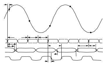
tA
|
|
|
|
N+3 |
|
|
N |
|
|
|
|
AIN |
|
|
|
|
|
|
|
N+1 |
|
|
|
|
|
|
N+2 |
|
|
|
|
tENCH |
tENCL |
|
N+4 |
|
|
tENC |
|
|
|
ENC, ENC |
N |
N+1 |
N+2 |
N+3 |
N+4 |
tE_RL |
|
tE_FL |
tE_DR |
tS_E |
tH_E |
D[13:0], OVR |
|
Nñ3 |
Nñ2 |
Nñ1 |
N |
 tH_DR
tH_DR 
tS_DR
DRY
tDR
Figure 1. Timing Diagram
–4– |
REV. 0 |

AD6645
ABSOLUTE MAXIMUM RATINGS*
Parameter |
Min |
Max |
Unit |
|
|
|
|
ELECTRICAL |
|
|
|
AVCC Voltage |
0 |
7 |
V |
DVCC Voltage |
0 |
7 |
V |
Analog Input Voltage |
0 |
AVCC |
V |
Analog Input Current |
|
25 |
mA |
Digital Input Voltage |
0 |
AVCC |
V |
Digital Output Current |
|
4 |
mA |
|
|
|
|
ENVIRONMENTAL |
|
|
∞C |
Operating Temperature Range (Ambient) |
–40 |
+85 |
|
Maximum Junction Temperature |
|
150 |
∞C |
Lead Temperature (Soldering, 10 sec) |
|
300 |
∞C |
Storage Temperature Range (Ambient) |
–65 |
+150 |
∞C |
*Absolute maximum ratings are limiting values to be applied individually and beyond which the serviceability of the circuit may be impaired. Functional operability is not necessarily implied. Exposure to absolute maximum rating conditions for an extended period of time may affect device reliability.
THERMAL CHARACTERISTICS |
EXPLANATION OF TEST LEVELS |
|||||||||
52-Lead PowerQuad 4 . . |
. . |
. . . |
. . . . . . . . . . . . . . . LQFP_ED |
Test Level |
|
|
||||
JA = 23∞C/W . . . . . . . |
. . . |
. . |
. . . Soldered Slug, No Airflow |
I. |
100% production tested. |
|
|
|||
JA = 17∞C/W . . . . . . . . |
|
Soldered Slug, 200 LFPM Airflow |
II. |
100% production tested at 25∞C and guaranteed by design |
||||||
JA = 30∞C/W . . . . . . . . |
. . |
. . |
. Unsoldered Slug, No Airflow |
|
and characterization at temperature extremes. |
|||||
JA = 24∞C/W . . . . . . |
Unsoldered Slug, 200 LFPM Airflow |
III. Sample tested only. |
|
|
||||||
JC = 2∞C/W . . . . . . . . . |
. . |
. . |
Bottom of Package (Heatslug) |
IV. Parameter is guaranteed by design and characterization |
||||||
Typical Four-Layer JEDEC Board Horizontal Orientation |
|
testing. |
|
|
||||||
V. |
Parameter is a typical value only. |
|||||||||
|
|
|
|
|
|
|||||
|
|
|
|
ORDERING GUIDE |
|
|
||||
|
|
|
|
|
|
|
|
|
||
|
Model |
|
|
Temperature Range |
|
Package Description |
Package Option |
|||
|
|
|
|
|
|
|
||||
|
AD6645ASQ-80 |
–40∞C to +85∞C (Ambient) |
|
52-Lead PowerQuad 4 (LQFP_ED) |
SQ-52 |
|||||
|
AD6645/PCB |
|
25∞C |
|
Evaluation Board |
|
|
|||
CAUTION
ESD (electrostatic discharge) sensitive device. Electrostatic charges as high as 4000 V readily accumulate on the human body and test equipment and can discharge without detection. Although the AD6645 features proprietary ESD protection circuitry, permanent damage may occur on devices subjected to high-energy electrostatic discharges. Therefore, proper ESD precautions are recommended to avoid performance degradation or loss of functionality.
WARNING! |
ESD SENSITIVE DEVICE |
REV. 0 |
–5– |
AD6645
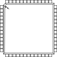
PIN CONFIGURATION
|
|
|
DRY |
D13(MSB) |
D12 |
|
D11 |
D10 |
D9 |
D8 |
D7 |
D6 |
DV |
GND |
D5 |
D4 |
|
|
|
|
|
|
|
|
|
|
|
|
|
|
CC |
|
|
|
|
|
|
|
52 |
51 |
50 |
|
49 |
48 |
47 |
46 |
45 |
44 |
43 |
42 |
41 |
40 |
|
|
|
DVCC |
1 |
PIN 1 |
|
|
|
|
|
|
|
|
|
|
39 |
D3 |
|
|
|
GND |
2 |
IDENTIFIER |
|
|
|
|
|
|
|
|
38 |
D2 |
|||
|
|
VREF |
3 |
|
|
|
|
|
|
|
|
|
|
|
|
37 |
D1 |
|
|
GND |
4 |
|
|
|
|
|
|
|
|
|
|
|
|
36 |
D0 (LSB) |
|
|
ENC |
5 |
|
|
|
|
|
|
|
|
|
|
|
|
35 |
DMID |
|
|
ENC 6 |
|
|
|
|
|
AD6645 |
|
|
|
|
34 |
GND |
|||
|
|
GND |
7 |
|
|
|
|
|
TOP VIEW |
|
|
|
|
33 |
DVCC |
||
|
|
AVCC |
8 |
|
|
|
|
(Not to Scale) |
|
|
|
32 |
OVR |
||||
|
|
|
|
|
|
|
|
|
|
|
|
|
|
||||
|
|
AVCC |
9 |
|
|
|
|
|
|
|
|
|
|
|
|
31 |
DNC |
|
|
GND 10 |
|
|
|
|
|
|
|
|
|
|
|
|
30 |
AVCC |
|
|
|
AIN 11 |
|
|
|
|
|
|
|
|
|
|
|
|
29 |
GND |
|
|
|
AIN 12 |
|
|
|
|
|
|
|
|
|
|
|
|
28 |
AVCC |
|
|
|
GND 13 |
|
|
|
|
|
|
|
|
|
|
|
|
27 |
GND |
|
|
|
|
14 |
15 |
16 |
|
17 |
18 |
19 |
20 |
21 |
22 |
23 |
24 |
25 |
26 |
|
|
|
|
AV |
GND |
AV |
|
GND |
AV |
GND |
C1 |
GND |
AV |
GND |
C2 |
GND |
AV |
|
|
|
|
CC |
|
CC |
|
CC |
|
|
|
CC |
|
|
|
CC |
|
|
|
|
|
|
|
|
DNC = DO NOT CONNECT |
|
|
|
||||||||
|
|
|
PIN FUNCTION DESCRIPTIONS |
||||||||||||||
|
|
|
|
|
|
|
|
|
|
|
|
|
|
|
|
|
|
Pin No. |
Mnemonic |
Function |
|
|
|
|
|
|
|
|
|
|
|
|
|
|
|
|
|
|
|||||||||||||||
1, 33, 43 |
DVCC |
3.3 V Power Supply (Digital) Output Stage Only |
|||||||||||||||
2, 4, 7, 10, 13, |
GND |
Ground |
|
|
|
|
|
|
|
|
|
|
|
|
|
|
|
15, 17, 19, 21, |
|
|
|
|
|
|
|
|
|
|
|
|
|
|
|
|
|
23, 25, 27, 29, |
|
|
|
|
|
|
|
|
|
|
|
|
|
|
|
|
|
34, 42 |
|
|
|
|
|
|
|
|
|
|
|
|
|
|
|
|
|
3 |
VREF |
2.4 V Reference. Bypass to ground with a 0.1 mF microwave chip capacitor. |
|||||||||||||||
5 |
ENC |
Encode Input. Conversion initiated on rising edge. |
|||||||||||||||
6 |
ENC |
Complement of ENC, Differential Input |
|
||||||||||||||
8, 9, 14, 16, 18, |
AVCC |
5 V Analog Power Supply |
|
|
|
|
|
|
|
||||||||
22, 26, 28, 30 |
|
|
|
|
|
|
|
|
|
|
|
|
|
|
|
|
|
11 |
AIN |
Analog Input |
|
|
|
|
|
|
|
|
|
|
|
|
|
||
12 |
AIN |
Complement of AIN, Differential Analog Input |
|||||||||||||||
20 |
C1 |
Internal Voltage Reference. Bypass to ground with a 0.1 mF chip capacitor. |
|||||||||||||||
24 |
C2 |
Internal Voltage Reference. Bypass to ground with a 0.1 mF chip capacitor. |
|||||||||||||||
31 |
DNC |
Do not connect this pin. |
|
|
|
|
|
|
|
|
|||||||
32 |
OVR* |
Over-Range Bit. A logic-level high indicates analog input exceeds ±FS. |
|||||||||||||||
35 |
DMID |
Output Data Voltage Midpoint. Approximately equal to (DVCC)/2. |
|||||||||||||||
36 |
D0 (LSB) |
Digital Output Bit (Least Significant Bit); Two’s Complement |
|||||||||||||||
37–41, 44–50 |
D1–D5, D6–D12 |
Digital Output Bits in Two’s Complement |
|
||||||||||||||
51 |
D13 (MSB) |
Digital Output Bit (Most Significant Bit); Two’s Complement |
|||||||||||||||
52 |
DRY |
DataReady Output |
|
|
|
|
|
|
|
|
|
|
|||||
|
|
|
|
|
|
|
|
|
|
|
|
|
|
|
|
|
|
*The functionality of the Over-Range bit is specified for a temperature range of 25∞C to 85∞C only.
–6– |
REV. 0 |
Loading...