


 Loading...
Analog Devices AD667SE, AD667SD, AD667KP, AD667JP, AD667JN Datasheet
...
a |
Microprocessor-Compatible |
|
12-Bit D/A Converter |
||
|
|
|
|
|
AD667* |
|
|
|
|
FEATURES |
FUNCTIONAL BLOCK DIAGRAM |
|
Complete 12-Bit D/A Function |
|
|
Double-Buffered Latch |
|
|
On Chip Output Amplifier |
|
|
High Stability Buried Zener Reference |
|
|
Single Chip Construction |
|
|
Monotonicity Guaranteed Over Temperature |
|
|
Linearity Guaranteed Over Temperature: 1/2 LSB max |
|
|
Settling Time: 3 ms max to 0.01% |
|
|
Guaranteed for Operation with 612 V or 615 V |
|
|
Supplies |
|
|
Low Power: 300 mW Including Reference |
|
|
TTL/5 V CMOS Compatible Logic Inputs |
|
|
Low Logic Input Currents |
|
|
MIL-STD-883 Compliant Versions Available |
|
PRODUCT DESCRIPTION
The AD667 is a complete voltage output 12-bit digital-to-analog converter including a high stability buried Zener voltage reference and double-buffered input latch on a single chip. The converter uses 12 precision high speed bipolar current steering switches and a laser trimmed thin-film resistor network to provide fast settling time and high accuracy.
Microprocessor compatibility is achieved by the on-chip doublebuffered latch. The design of the input latch allows direct interface to 4-, 8-, 12-, or 16-bit buses. The 12 bits of data from the first rank of latches can then be transferred to the second rank, avoiding generation of spurious analog output values. The latch responds to strobe pulses as short as 100 ns, allowing use with the fastest available microprocessors.
The functional completeness and high performance in the AD667 results from a combination of advanced switch design, high speed bipolar manufacturing process, and the proven laser wafer-trimming (LWT) technology. The AD667 is trimmed at the wafer level and is specified to ±1/4 LSB maximum linearity error (K, B grades) at +25°C and ±1/2 LSB over the full operating temperature range.
The subsurface (buried) Zener diode on the chip provides a low noise voltage reference which has long-term stability and temperature drift characteristics comparable to the best discrete reference diodes. The laser trimming process which provides the excellent linearity, is also used to trim the absolute value of the reference as well as its temperature coefficient. The AD667 is thus well suited for wide temperature range performance with
±1/2 LSB maximum linearity error and guaranteed monotonicity over the full temperature range. Typical full-scale gain TC is 5 ppm/°C.
*Protected by Patent Numbers 3,803,590; 3,890,611; 3,932,863; 3,978,473; 4,020,486; and others pending.
REV. A
Information furnished by Analog Devices is believed to be accurate and reliable. However, no responsibility is assumed by Analog Devices for its use, nor for any infringements of patents or other rights of third parties which may result from its use. No license is granted by implication or otherwise under any patent or patent rights of Analog Devices.
The AD667 is available in five performance grades. The AD667J and K are specified for use over the 0°C to +70°C temperature range and are available in a 28-pin molded plastic DIP
(N) or PLCC (P) package. The AD667S grade is specified for the –55°C to +125°C range and is available in the ceramic DIP
(D) or LCC (E) package. The AD667A and B are specified for use over the –25°C to +85°C temperature range and are available in a 28-pin hermetically sealed ceramic DIP (D) package.
PRODUCT HIGHLIGHTS
1.The AD667 is a complete voltage output DAC with voltage reference and digital latches on a single IC chip.
2.The double-buffered latch structure permits direct interface to 4-, 8-, 12-, or 16-bit data buses. All logic inputs are TTL or 5 volt CMOS compatible.
3.The internal buried Zener reference is laser-trimmed to 10.00 volts with a ±1% maximum error. The reference voltage is also available for external application.
4.The gain setting and bipolar offset resistors are matched to the internal ladder network to guarantee a low gain temperature coefficient and are laser-trimmed for minimum full-scale and bipolar offset errors.
5.The precision high speed current steering switch and on-board
high speed output amplifier settle within 1/2 LSB for a 10 V full-scale transition in 2.0 μs as when properly compensated.
6.The AD667 is available in versions compliant with MIL- STD-883. Refer to the Analog Devices Military Products Databook or current AD667/883B data sheet for detailed specifications.
One Technology Way, P.O. Box 9106, Norwood, MA 02062-9106, U.S.A. Tel: 617/329-4700 Fax: 617/326-8703
AD667–SPECIFICATIONS (@ TA = +258C, 612 V, 615 V power supplies unless otherwise noted)
Model |
|
AD667J |
|
|
AD667K |
|
|
|
Min |
Typ |
Max |
Min |
Typ |
Max |
Units |
|
|
|
|
|
|
|
|
DIGITAL INPUTS |
|
|
|
|
|
|
|
Resolution |
|
|
12 |
|
|
12 |
Bits |
Logic Levels (TTL, Compatible, TMIN–TMAX)1 |
+2.0 |
|
|
+2.0 |
|
|
|
VIH (Logic “l’’) |
|
+5.5 |
|
+5.5 |
V |
||
VIL (Logic “0”) |
0 |
|
+0.8 |
0 |
|
+0.8 |
V |
IIH (VIH = 5.5 V) |
|
3 |
10 |
|
3 |
10 |
μA |
IIL (VIL = 0.8 V) |
|
1 |
5 |
|
1 |
5 |
μA |
TRANSFER CHARACTERISTICS |
|
|
|
|
|
|
|
ACCURACY |
|
|
|
|
± 1/8 |
|
|
Linearity Error @ +25°C |
|
+1/4 |
61/2 |
|
61/4 |
LSB |
|
TA = TMIN to TMAX |
|
± 1/2 |
63/4 |
|
± 1/4 |
61/2 |
LSB |
Differential Linearity Error @ +25°C |
|
± 1/2 |
63/4 |
|
± 1/4 |
61/2 |
LSB |
TA = TMIN to TMAX |
Monotonicity Guaranteed |
|
Monotonicity Guaranteed |
LSB |
|||
Gain Error2 |
|
± 0.1 |
60.2 |
|
± 0.1 |
60.2 |
% FSR3 |
Unipolar Offset Error2 |
|
± 1 |
62 |
|
± 1 |
62 |
LSB |
Bipolar Zero2 |
|
± 0.05 |
60.1 |
|
± 0.05 |
60.1 |
% of FSR |
DRIFT |
|
± 2 |
|
|
± 2 |
|
ppm of FSR/°C |
Differential Linearity |
|
|
|
|
|||
Gain (Full Scale) TA = 25°C to TMIN or TMAX |
|
± 5 |
± 30 |
|
± 5 |
± 15 |
ppm of FSR/°C |
Unipolar Offset TA = –25°C to TMIN or TMAX |
|
± 1 |
± 3 |
|
|
± 3 |
ppm of FSR/°C |
Bipolar Zero TA = 25°C to TMIN or TMAX |
|
± 5 |
± 10 |
|
|
± 10 |
ppm of FSR/°C |
CONVERSION SPEED |
|
|
|
|
|
|
|
Settling Time to ± 0.01% of FSR for |
|
|
|
|
|
|
|
FSR Change (2 kΩi500 pF Load) |
|
|
|
|
|
|
μs |
with 10 kΩ Feedback |
|
3 |
4 |
|
3 |
4 |
|
with 5 kΩ Feedback |
|
2 |
3 |
|
2 |
3 |
μs |
For LSB Change |
|
1 |
|
|
1 |
|
μs |
Slew Rate |
10 |
|
|
10 |
|
|
V/μs |
ANALOG OUTPUT |
|
± 2.5, ±5, ± 10, |
|
|
± 2.5, ±5, ±10, |
|
|
Ranges4 |
|
|
|
|
V |
||
|
± 5 |
+5, +10 |
|
± 5 |
+5, +10 |
|
|
Output Current |
|
|
|
|
mA |
||
Output Impedance (DC) |
|
0.05 |
|
|
0.05 |
|
Ω |
Short Circuit Current |
|
|
40 |
|
|
40 |
mA |
REFERENCE OUTPUT |
9.90 |
10.00 |
10.10 |
9.90 |
10.00 |
10.10 |
V |
External Current |
0.1 |
1.0 |
|
0.1 |
1.0 |
|
mA |
POWER SUPPLY SENSITIVITY |
|
|
|
|
|
|
|
VCC = +11.4 V to +16.5 V dc |
|
5 |
10 |
|
5 |
10 |
ppm of FS/% |
VEE = –11.4 V to –16.5 V dc |
|
5 |
10 |
|
5 |
10 |
ppm of FS/% |
POWER SUPPLY REQUIREMENTS |
|
± 12, ± 15 |
|
|
± 12, ± 15 |
|
|
Rated Voltages |
|
|
|
|
V |
||
Range4 |
611.4 |
|
616.5 |
611.4 |
|
616.5 |
V |
Supply Current |
|
|
|
|
|
|
|
+11.4 V to +16.5 V dc |
|
8 |
12 |
|
8 |
12 |
mA |
–11.4 V to –16.5 V dc |
|
20 |
25 |
|
20 |
25 |
mA |
TEMPERATURE RANGE |
|
|
|
|
|
|
°C |
Specification |
0 |
|
+70 |
0 |
|
+70 |
|
Storage |
–65 |
|
+125 |
–65 |
|
+125 |
°C |
NOTES
1The digital input specifications are 100% tested at +25°C, and guaranteed but not tested over the full temperature range. 2Adjustable to zero.
3FSR means “Full-Scale Range” and is 20 V for ±10 V range and 10 V for the ±5 V range.
4A minimum power supply of ±12.5 V is required for a ±10 V full-scale output and ±11.4 V is required for all other voltage ranges.
Specifications subject to change without notice.
Specifications shown in boldface are tested on all production units at final electrical test. Results from those tests are used to calculate outgoing quality levels. All min and max specifications are guaranteed, although only those shown in boldface are tested on all production units.
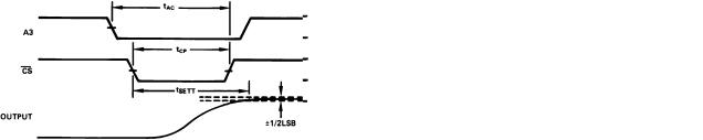
TIMING SPECIFICATIONS
(All Models, TA = +25°C, VCC = +12 V or +15 V, VEE = –12 V or –15 V)
Symbol |
|
Parameter |
Min |
Typ |
Max |
|
|||||
|
|
|
|
|
|
|
|
|
|
|
|
tDC |
|
Data Valid to End of |
|
|
|
|
50 |
– |
– |
ns |
|
CS |
|||||||||||
tAC |
|
Address Valid to End of |
CS |
|
100 |
_ |
_ |
ns |
|||
tCP |
|
CS |
Pulse Width |
100 |
– |
– |
ns |
||||
tDH |
|
Data Hold Time |
0 |
– |
– |
ns |
|||||
tSETT |
|
Output Voltage Settling Time |
– |
2 |
4 |
μs |
|||||
ABSOLUTE MAXIMUM RATINGS
VCC to Power Ground . . . . . . . . . . . . . . . . . . . . . 0 V to +18 V VEE to Power Ground . . . . . . . . . . . . . . . . . . . . . 0 V to –18 V Digital Inputs (Pins 11–15, 17–28)
to Power Ground . . . . . . . . . . . . . . . . . . . . –1.0 V to +7.0 V Ref In to Reference Ground . . . . . . . . . . . . . . . . . . . . . . ±12 V Bipolar Offset to Reference Ground . . . . . . . . . . . . . . . . ±12 V 10 V Span R to Reference Ground . . . . . . . . . . . . . . . . . ±12 V 20 V Span R to Reference Ground . . . . . . . . . . . . . . . . . ±24 V Ref Out, VOUT (Pins 6, 9) . . Indefinite Short to Power Ground
. . . . . . . . . . . . . . . . . . . . . . . . . . . Momentary Short to VCC Power Dissipation . . . . . . . . . . . . . . . . . . . . . . . . . . 1000 mW
–2– |
REV. A |
|
|
|
|
|
|
|
|
|
|
AD667 |
|
|
|
|
|
|
|
|
|
|
|
Model |
|
AD667A |
|
|
AD667B |
|
|
AD667S |
|
|
|
Min |
Typ |
Max |
Min |
Typ |
Max |
Min |
Typ |
Max |
Units |
|
|
|
|
|
|
|
|
|
|
|
DIGITAL INPUTS |
|
|
|
|
|
|
|
|
|
|
Resolution |
|
|
12 |
|
|
12 |
|
|
12 |
Bits |
Logic Levels (TTL, Compatible, TMIN–TMAX)1 |
+2.0 |
|
+5.5 |
+2.0 |
|
+5.5 |
+2.0 |
|
+5.5 |
|
VIH (Logic “l’’) |
|
|
|
V |
||||||
VIL (Logic “0”) |
0 |
|
+0.8 |
0 |
|
+0.8 |
0 |
|
+0.7 |
V |
IIH (VIH = 5.5 V) |
|
3 |
10 |
|
3 |
10 |
|
3 |
10 |
μA |
IIL (VIL = 0.8 V) |
|
1 |
5 |
|
1 |
5 |
|
1 |
5 |
μA |
TRANSFER CHARACTERISTICS |
|
|
|
|
|
|
|
|
|
|
ACCURACY |
|
|
|
|
|
|
|
|
|
|
Linearity Error @ +25°C |
|
+1/4 |
61/2 |
|
± 1/8 |
61/4 |
|
± 1/8 |
61/2 |
LSB |
TA = TMIN to TMAX |
|
± 1/2 |
63/4 |
|
± 1/4 |
61/2 |
|
± 1/8 |
63/4 |
LSB |
Differential Linearity Error @ +25°C |
|
± 1/2 |
63/4 |
|
± 1/4 |
61/2 |
|
± 1/4 |
63/4 |
LSB |
TA = TMIN to TMAX |
Monotonicity Guaranteed |
Monotonicity Guaranteed |
Monotonicity Guaranteed |
LSB |
||||||
Gain Error2 |
|
± 0.1 |
60.2 |
|
± 0.1 |
60.2 |
|
± 0.1 |
60.2 |
% FSR3 |
Unipolar Offset Error2 |
|
± 1 |
62 |
|
± 1 |
62 |
|
± 1 |
62 |
LSB |
Bipolar Zero2 |
|
± 0.05 |
60.1 |
|
± 0.05 |
60.1 |
|
± 0.05 |
60.1 |
% of FSR |
DRIFT |
|
± 2 |
|
|
± 2 |
|
|
± 2 |
|
ppm of FSR/°C |
Differential Linearity |
|
|
|
|
|
|
||||
Gain (Full Scale) TA = 25°C to TMIN or TMAX |
|
± 5 |
± 30 |
|
± 5 |
± 15 |
|
± 15 |
630 |
ppm of FSR/°C |
Unipolar Offset TA = 25°C to TMIN or TMAX |
|
± 1 |
± 3 |
|
|
± 3 |
|
|
63 |
ppm of FSR/°C |
Bipolar Zero TA = 25°C to TMIN or TMAX |
|
± 5 |
± 10 |
|
|
± 10 |
|
|
610 |
ppm of FSR/°C |
CONVERSION SPEED |
|
|
|
|
|
|
|
|
|
|
Settling Time to ±0.01% of FSR for |
|
|
|
|
|
|
|
|
|
|
FSR Change (2 kΩi500 pF Load) |
|
|
|
|
|
|
|
|
|
|
with 10 kΩ Feedback |
|
3 |
4 |
|
3 |
4 |
|
3 |
4 |
μs |
with 5 kΩ Feedback |
|
2 |
3 |
|
2 |
3 |
|
2 |
3 |
μs |
For LSB Change |
|
1 |
|
|
1 |
|
|
1 |
|
μs |
Slew Rate |
10 |
|
|
10 |
|
|
10 |
|
|
V/μs |
ANALOG OUTPUT |
|
± 2.5, ±5, ±10, |
|
± 2.5, ± 5, ±10, |
|
± 2.5, ± 5, ±10, |
|
|||
Ranges4 |
|
|
|
V |
||||||
|
± 5 |
+5, +10 |
|
± 5 |
+5, +10 |
|
± 5 |
+5, +10 |
|
|
Output Current |
|
|
|
|
|
|
mA |
|||
Output Impedance (DC) |
|
0.05 |
|
|
0.05 |
|
|
0.05 |
|
Ω |
Short Circuit Current |
|
|
40 |
|
|
40 |
|
|
40 |
mA |
REFERENCE OUTPUT |
9.90 |
10.00 |
10.10 |
9.90 |
10.00 |
10.10 |
9.90 |
10.00 |
10.10 |
V |
External Current |
0.1 |
1.0 |
|
0.1 |
1.0 |
|
1.0 |
|
|
mA |
POWER SUPPLY SENSITIVITY |
|
|
|
|
|
|
|
|
|
|
VCC = +11.4 V to +16.5 V dc |
|
5 |
10 |
|
5 |
10 |
|
5 |
10 |
ppm of FS/% |
VEE = –11.4 V to –16.5 V dc |
|
5 |
10 |
|
5 |
10 |
|
5 |
10 |
ppm of FS/% |
POWER SUPPLY REQUIREMENTS |
|
± 12, ± 15 |
|
|
± 12, ± 15 |
|
|
± 12, ± 15 |
|
|
Rated Voltages |
|
|
|
|
|
|
V |
|||
Range4 |
611.4 |
|
616.5 |
611.4 |
|
616.5 |
611.4 |
|
616.5 |
V |
Supply Current |
|
|
|
|
|
|
|
|
|
|
+11.4 V to +16.5 V dc |
|
8 |
12 |
|
8 |
12 |
|
8 |
12 |
mA |
–11.4 V to –16.5 V dc |
|
20 |
25 |
|
20 |
25 |
|
20 |
25 |
mA |
TEMPERATURE RANGE |
|
|
|
|
|
|
|
|
|
°C |
Specification |
–25 |
|
+85 |
–25 |
|
+85 |
–55 |
|
+125 |
|
Storage |
–65 |
|
+150 |
–65 |
|
+150 |
–65 |
|
+150 |
°C |
TIMING DIAGRAMS |
|
|
|
WRITE CYCLE #2 |
|
|
|
|
||
WRITE CYCLE #1 |
|
|
|
(Load Second Rank from First Rank; A2, A1, A0 = 1) |
||||||
(Load First Rank from Data Bus; A3 = 1)
REV. A |
–3– |
Loading...