


 Loading...
Analog Devices AD664KP, AD664KN-UNI, AD664KN-BIP, AD664JP, AD664JN-BIP Datasheet
...a |
Monolithic |
|
12-Bit Quad DAC |
||
|
|
|
|
|
AD664 |
|
|
|
FEATURES
Four Complete Voltage Output DACs Data Register Readback Feature “Reset to Zero” Override Multiplying Operation Double-Buffered Latches
Surface Mount and DIP Packages MIL-STD-883 Compliant Versions Available
APPLICATIONS
Automatic Test Equipment
Robotics
Process Control
Disk Drives
Instrumentation
Avionics
PRODUCT DESCRIPTION
The AD664 is four complete 12-bit, voltage-output DACs on one monolithic IC chip. Each DAC has a double-buffered input latch structure and a data readback function. All DAC read and write operations occur through a single microprocessor-compatible I/O port.
The I/O port accommodates 4-, 8- or 12-bit parallel words allowing simple interfacing with a wide variety of microprocessors. A reset to zero control pin is provided to allow a user to simultaneously reset all DAC outputs to zero, regardless of the contents of the input latch. Any one or all of the DACs may be placed in a transparent mode allowing immediate response by the outputs to the input data.
The analog portion of the AD664 consists of four DAC cells, four output amplifiers, a control amplifier and switches. Each DAC cell is an inverting R-2R type. The output current from each DAC is switched to the on-board application resistors and output amplifier. The output range of each DAC cell is programmed through the digital I/O port and may be set to unipolar or bipolar range, with a gain of one or two times the reference voltage. All DACs are operated from a single external reference.
The functional completeness of the AD664 results from the combination of Analog Devices’ BiMOS II process, laser-trimmed thin-film resistors and double-level metal interconnects.
PRODUCT HIGHLIGHTS
1.The AD664 provides four voltage-output DACs on one chip offering the highest density 12-bit D/A function available.
2.The output range of each DAC is fully and independently programmable.
3.Readback capability allows verification of contents of the internal data registers.
REV. C
Information furnished by Analog Devices is believed to be accurate and reliable. However, no responsibility is assumed by Analog Devices for its use, nor for any infringements of patents or other rights of third parties which may result from its use. No license is granted by implication or otherwise under any patent or patent rights of Analog Devices.
PIN CONFIGURATIONS
44-Pin Package
28-Pin DIP Package
4.The asynchronous RESET control returns all D/A outputs to zero volts.
5.DAC-to-DAC matching performance is specified and tested.
6.Linearity error is specified to be 1/2 LSB at room temperature and 3/4 LSB maximum for the K, B and T grades.
7.DAC performance is guaranteed to be monotonic over the full operating temperature range.
8.Readback buffers have tristate outputs.
9.Multiplying-mode operation allows use with fixed or variable, positive or negative external references.
10.The AD664 is available in versions compliant with MIL- STD-883. Refer to the Analog Devices Military Products Databook or current AD664/883B data sheet for detailed specifications.
One Technology Way, P.O. Box 9106, Norwood, MA 02062-9106, U.S.A. Tel: 617/329-4700 Fax: 617/326-8703
|
|
(VLL = +5 V, VCC = +15 V, VEE = –15 V, VREF = +10 V, TA = +258C |
|
|
|||||
AD664–SPECIFICATIONS unless otherwise noted) |
|
|
|
|
|
||||
|
Model |
|
JN/JP/AD/AJ/SD |
KN/KP/BD/BJ/BE/TD/TE |
|
||||
|
|
|
Min |
Typ |
Max |
Min |
Typ |
Max |
Units |
|
|
|
|
|
|
|
|
|
|
|
RESOLUTION |
|
|
12 |
12 |
|
* |
* |
Bits |
|
|
|
|
|
|
|
|
|
|
|
ANALOG OUTPUT |
|
|
|
|
|
|
|
|
|
Voltage Range1 |
|
|
|
|
|
|
|
|
|
UNI Versions |
|
0 |
|
VCC – 2.02 |
* |
|
* |
Volts |
|
BIP Versions |
|
VEE + 2.02 |
|
VCC – 2.02 |
* |
|
* |
Volts |
|
Output Current |
|
5 |
|
|
* |
|
|
mA |
|
Load Resistance |
|
|
2 |
|
|
* |
|
kΩ |
|
Load Capacitance |
|
|
|
500 |
|
|
* |
pF |
|
Short-Circuit Current |
|
|
25 |
40 |
|
* |
* |
mA |
|
|
|
|
|
|
|
|
|
|
|
ACCURACY |
|
|
±3 |
|
|
±2 |
|
|
|
Gain Error |
|
–7 |
7 |
–5 |
5 |
LSB |
||
|
Unipolar Offset |
|
–2 |
±1/2 |
2 |
–1 |
±1/4 |
1 |
LSB |
|
Bipolar Zero3 |
|
–3 |
±3/4 |
3 |
–2 |
±1/2 |
2 |
LSB |
|
Linearity Error4 |
|
–3/4 |
±1/2 |
3/4 |
–1/2 |
±1/4 |
1/2 |
LSB |
|
Linearity TMIN to TMAX |
|
–1 |
±3/4 |
1 |
–3/4 |
±1/2 |
3/4 |
LSB |
|
Differential Linearity |
|
–3/4 |
|
3/4 |
–1/2 |
|
1/2 |
LSB |
|
Differential Linearity TMIN to TMAX |
|
Monotonic @ All Temperatures |
Monotonic @ All Temperatures |
|
||||
|
Gain Error Drift |
|
|
±7 |
|
|
±5 |
|
ppm of FSR5/°C |
|
Unipolar 0 V to +10 V Mode |
|
–12 |
12 |
–10 |
10 |
|||
|
Bipolar –5 V to +5 V Mode |
|
–12 |
±7 |
12 |
–10 |
±5 |
10 |
ppm of FSR/°C |
|
Bipolar –10 V to +10 V Mode |
|
–12 |
±7 |
12 |
–10 |
±5 |
10 |
ppm of FSR/°C |
|
Unipolar Offset Drift |
|
|
±l.5 |
|
|
±l |
|
ppm of FSR/°C |
|
Unipolar 0 V to +10 V Mode |
|
–3 |
3 |
–2 |
2 |
|||
|
Bipolar Zero Drift |
|
|
±7 |
|
|
±5 |
|
ppm of FSR/°C |
|
Bipolar –5 V to +5 V Mode |
|
–12 |
12 |
–10 |
10 |
|||
|
Bipolar –10 V to +10 V Mode |
|
–12 |
±7 |
12 |
–10 |
±5 |
10 |
ppm of FSR/°C |
|
|
|
|
|
|
|
|
|
|
|
REFERENCE INPUT |
|
|
|
|
|
|
|
kΩ |
|
Input Resistance |
|
1.3 |
|
2. 6 |
* |
|
* |
|
|
Voltage Range6 |
|
VEE + 2.02 |
|
VCC – 2.02 |
* |
|
* |
Volts |
|
POWER REOUIREMENTS |
|
|
|
|
|
|
|
|
|
VLL |
|
4.5 |
5.0 |
5.5 |
* |
* |
* |
Volts |
|
ILL |
|
|
|
|
|
|
|
|
|
@ VIH, VIL = 5 V, 0 V |
|
|
0.1 |
1 |
|
* |
* |
mA |
|
@ VIH, VIL = 2.4 V, 0.4 V |
|
|
3 |
6 |
|
* |
* |
mA |
|
VCC /VEE |
|
611.4 |
|
616.5 |
* |
|
* |
Volts |
|
ICC |
|
|
12 |
15 |
|
* |
* |
mA |
|
IEE |
|
|
15 |
19 |
|
* |
* |
mA |
|
Total Power |
|
|
400 |
525 |
|
* |
* |
mW |
|
|
|
|
|
|
|
|
|
|
|
ANALOG GROUND CURRENT7 |
|
–600 |
±400 |
+600 |
* |
* |
* |
μA |
|
MATCHING PERFORMANCE |
|
|
±3 |
|
|
±2 |
|
|
|
Gain8 |
|
–6 |
6 |
–4 |
4 |
LSB |
||
|
Offset9 |
|
–2 |
±1/2 |
2 |
–1 |
±1/4 |
1 |
LSB |
|
Bipolar Zero10 |
|
–3 |
±1 |
3 |
–2 |
±1 |
2 |
LSB |
|
Linearity11 |
|
–1.5 |
±1/2 |
1.5 |
–1 |
±1/2 |
1 |
LSB |
|
CROSSTALK |
|
|
|
|
|
|
|
|
|
Analog |
|
|
|
–90 |
|
|
* |
dB |
|
Digital |
|
|
|
–60 |
|
|
* |
dB |
|
|
|
|
|
|
|
|
|
|
|
DYNAMIC PERFORMANCE (RL = 2 kΩ, CL = 500 pF) |
|
|
|
|
|
|
|
|
|
Settling Time to ±1/2 LSB |
|
|
|
|
|
|
|
|
|
Off←Bits→On, GAIN = 1, VREF = 10 |
|
|
8 |
10 |
|
* |
* |
μs |
|
Settling Time to ±1/2 LSB |
|
|
|
|
|
|
|
|
|
–10←VREF →10 V, GAIN = 1, Bits On |
|
|
10 |
|
|
* |
|
μs |
|
Glitch Impulse |
|
|
|
500 |
|
|
* |
nV-sec |
|
|
|
|
|
|
|
|
|
|
|
MULTIPLYING MODE PERFORMANCE |
|
|
|
|
|
|
|
|
|
Reference Feedthrough @ 1 kHz |
|
|
–75 |
|
|
* |
|
dB |
|
Reference –3 dB Bandwidth |
|
|
70 |
|
|
* |
|
kHz |
|
|
|
|
|
|
|
|
|
|
|
POWER SUPPLY GAIN SENSITIVITY |
|
|
|
|
|
|
|
|
|
11.4 V←VCC→16.5 V |
|
|
±2 |
65 |
|
* |
* |
ppm/% |
|
–16.5 V←VEE→–11.4 V |
|
|
±2 |
65 |
|
* |
* |
ppm/% |
|
4.5 V←VLL→5.5 V |
|
|
±2 |
65 |
|
* |
* |
ppm/% |
–2– |
REV. C |

|
|
|
|
|
|
|
|
|
|
|
|
|
|
|
|
|
|
|
|
|
|
|
AD664 |
|
|
|
|
|
|
|
|
|
|
|
|
|
|
|
|
|
|
|
|
|
|||
Model |
|
|
JN/JP/AD/AJ/SD |
KN/KP/BD/BJ/BE/TD/TE |
|
||||||||||||||||||
|
|
|
|
|
|
|
|
|
|
|
|
|
|
|
|
|
Min |
Typ |
Max |
Min |
Typ |
Max |
Units |
|
|
|
|
|
|
|
|
|
|
|
|
|
|
|
|
|
|
|
|
|
|
|
|
DIGITAL INPUTS |
|
|
|
|
|
|
|
|
|||||||||||||||
|
VIH |
|
2.0 |
|
|
* |
|
|
Volts |
||||||||||||||
|
VIL |
|
0 |
|
0.8 |
* |
|
* |
Volts |
||||||||||||||
|
Data Inputs |
|
|
±1 |
|
|
|
|
μA |
||||||||||||||
|
IIH @ VIN = VLL |
|
–10 |
10 |
* |
* |
* |
||||||||||||||||
|
IIL @ VIN = DGND |
|
–10 |
±1 |
10 |
* |
* |
* |
μA |
||||||||||||||
|
CS |
/DS0/DS1/ |
RST |
/ |
RD |
/ |
LS |
|
|
±1 |
|
|
|
|
μA |
||||||||
|
IIH @ VIN = VLL |
|
–10 |
10 |
* |
* |
* |
||||||||||||||||
|
IIL @ VIN = VLL |
|
–10 |
±1 |
10 |
* |
* |
* |
μA |
||||||||||||||
|
MS |
/ |
TR |
12 |
|
|
|
|
|
|
|
|
|
μA |
|||||||||
|
IIH @ VIN = VLL |
|
–10 |
5 |
10 |
* |
* |
* |
|||||||||||||||
|
IIL @ VIN = DGND |
|
–10 |
–5 |
0 |
* |
* |
* |
μA |
||||||||||||||
|
QS0 |
/ |
QSl |
/ |
QS2 |
l2 |
|
|
|
|
|
|
|
μA |
|||||||||
|
IIH @ VIN = VLL |
|
–10 |
5 |
10 |
* |
* |
* |
|||||||||||||||
|
IIL @ VIN = DGND |
|
–10 |
±1 |
10 |
* |
* |
* |
μA |
||||||||||||||
|
|
|
|
|
|
|
|
|
|||||||||||||||
DIGITAL OUTPUTS |
|
|
|
|
|
|
|
|
|||||||||||||||
|
VOL @ 1.6 mA Sink |
|
|
|
0.4 |
|
|
* |
Volts |
||||||||||||||
|
VOH @ 0.5 mA Source |
|
2.4 |
|
|
* |
|
|
Volts |
||||||||||||||
TEMPERATURE RANGE |
|
|
|
|
|
|
|
°C |
|||||||||||||||
|
JN/JP/KN/KP |
|
0 |
|
+70 |
* |
|
* |
|||||||||||||||
|
AD/AJ/BD/BJ/BE |
|
– 40 |
|
+85 |
* |
|
* |
°C |
||||||||||||||
|
SD/TD/TE |
|
–55 |
|
+125 |
* |
|
* |
°C |
||||||||||||||
|
|
|
|
|
|
|
|
|
|
|
|
|
|
|
|
|
|
|
|
|
|
|
|
NOTES
1A minimum power supply of ±12.0 V is required for 0 V to +10 V and ±10 V operation. A minimum power supply of ±11.4 V is required for –5 V to +5 V operation. 2For VCC < +12 V and VEE > –12 V. Voltage not to exeeed 10 V maximum.
3Bipolar zero error is the difference from the ideal output (0 volts) and the actual output voltage with code 100 000 000 000 applied to the inputs. 4Linearity error is defined as the maximum deviation of the actual DAC output from the ideal output (a straight line drawn from 0 to F.S. – 1 LSB). 5FSR means Full-Scale Range and is 20 V for ±10 V range and 10 V for ± 5 V range.
6A minimum power supply of ±12.0 V is required for a 10 V reference voltage. 7Analog Ground Current is input code dependent.
8Gain error matching is the largest difference in gain error between any two DACs in one package. 9Offset error matching is the largest difference in offset error between any two DACs in one package.
10Bipolar zero error matching is the largest difference in bipolar zero error between any two DACs in one package. 11Linearity error matching is the difference in the worst ease linearity error between any two DACs in one package. 1244-pin versions only.
*Specifications same as JN/JP/AD/AJ/SD. Specifications subject to change without notice.
Specifications shown in boldface are tested on all production units at final electrical test. Results from those tests are used to calculate outgoing quality levels. All min and max specifications are guaranteed, although only those shown in boldface are tested on all production units.
Digital Inputs . . . . . . . . . . . . . . . . . . . . . . . . . . –0.3 V to +7 V
Analog Outputs . . . . . . . . . . . . . . . . . . . . . Indefinite Shorts to
VCC, VLL, VEE and GND
*Stresses above those listed under “Absolute Maximum Ratings” may cause permanent damage to the device. This is a stress rating only and functional operation of the device at these or any other conditions above those indicated in the operational section of this specification is not implied. Exposure to absolute maximum rating conditions for extended periods may affect device reliability.
WARNING!
ESD SENSITIVE DEVICE
–3–

AD664
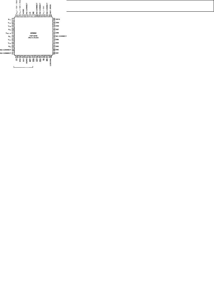
Figure 1a. 44-Pin Block Diagram
FUNCTIONAL DESCRIPTION
The AD664 combines four complete 12-bit voltage output D/A converters with a fast, flexible digital input/output port on one monolithic chip. It is available in two forms, a 44-pin version shown in Figure 1a and a 28-pin version shown in Figure 1b.
44-Pin Versions
Each DAC offers flexibility, accuracy and good dynamic performance. The R-2R structure is fabricated from thin-film resistors which are laser-trimmed to achieve 1/2 LSB linearity and guaranteed monotonicity. The output amplifier combines the best features of the bipolar and MOS devices to achieve good dynamic performance and low offset. Settling time is under 10 μs and each output can drive a 5 mA, 500 pF load. Short-circuit protection allows indefinite shorts to VLL, VCC, VEE and GND. The output and span resistor pins are available separately. This feature allows a user to insert current-boosting elements to increase the drive capability of the system, as well as to overcome parasitics.
Digital circuitry is implemented in CMOS logic. The fast, low power, digital interface allows the AD664 to be interfaced with most microprocessors. Through this interface, the wide variety of features on each chip may be accessed. For example, the input data for each DAC is programmed by way of 4-, 8-, 12or 16-bit words. The double-buffered input structure of this latch allows all four DACs to be updated simultaneously. A readback feature allows the internal registers to be read back through the same digital port, as either 4-, 8- or 12-bit words. When disabled, the readback drivers are placed in a high impedance (tristate) mode. A TRANSPARENT mode allows the input data to pass straight through both ranks of input registers and appear at the DAC with a minimum of delay. One D/A may be placed in the transparent mode at a time, or all four may be made transparent at once. The MODE SELECT feature allows the output range and mode of the DACs to be selected via the data bus inputs. An internal mode select register stores the selec-
tions. This register may also be read back to check its contents. A RESET-TO-ZERO feature allows all DACs to be reset to 0 volts out by strobing a single pin.
Figure 1b. 28-Pin Block Diagram
28-Pin Versions
The 28-pin versions are dedicated versions of the 44-pin AD664. Each offers a reduced set of features from those offered in the 44-pin version. This accommodates the reduced number of package pins available. Data is written and read with 12-bit words only. Output range and mode select functions are also not available in 28-pin versions. As an alternative, users specify
either the UNI (unipolar, 0 to VREF) models or the BIP (bipolar, –VREF to VREF) models depending on the application requirements. Finally, the transparent mode is not available on the 28-pin versions.
–4– |
REV. C |
AD664
Table I. Transfer Functions
|
|
Mode = UNI |
|
Mode = BIP |
|
|
|
|
|
|
|
|
|
|
|
000000000000 |
= 0 V |
000000000000 |
= – VREF/2 |
|
Gain = 1 |
100000000000 = VREF/2 |
100000000000 |
= 0 V |
|||
|
|
111111111111 |
= VREF – 1 LSB |
111111111111 |
= VREF/2 –1 LSB |
|
|
|
000000000000 |
= 0 V |
000000000000 |
= VREF |
|
Gain = 2 |
100000000000 = VREF |
100000000000 |
= 0 V |
|||
|
|
111111111111 |
= 2 × VREF – 1 LSB |
111111111111 |
= +VREF – 1 LSB |
|
DEFINITIONS OF SPECIFICATIONS
LINEARITY ERROR: Analog Devices defines linearity error as the maximum deviation of the actual, adjusted DAC output from the ideal analog output (a straight line drawn from 0 to FS
– 1 LSB) for any bit combination. This is also referred to as relative accuracy. The AD664 is laser-trimmed to typically maintain linearity errors at less than ±1/4 LSB.
MONOTONICITY: A DAC is said to be monotonic if the output either increases or remains constant for increasing digital inputs such that the output will always be a nondecreasing function of input. All versions of the AD664 are monotonic over their full operating temperature range.
DIFFERENTIAL LINEARITY: Monotonic behavior requires that the differential linearity error be less than 1 LSB both at 25°C as well as over the temperature range of interest. Differential nonlinearity is the measure of the variation in analog value, normalized to full scale, associated with a 1 LSB change in digital input code. For example, for a 10 V full-scale output, a change of 1 LSB in digital input code should result in a
2.44 mV change in the analog output (VREF = 10 V, Gain = 1, 1 LSB = 10 V × 1/4096 = 2.44 mV). If in actual use, however, a 1 LSB change in the input code results in a change of only 0.61 mV (1/4 LSB) in analog output, the differential nonlinearity error would be –1.83 mV, or –3/4 LSB.
GAIN ERROR: DAC gain error is a measure of the difference between the output span of an ideal DAC and an actual device.
UNIPOLAR OFFSET ERROR: Unipolar offset error is the difference between the ideal output (0 V) and the actual output of a DAC when the input is loaded with all “0s” and the MODE is unipolar.
BIPOLAR ZERO ERROR: Bipolar zero error is the difference between the ideal output (0 V) and the actual output of a DAC when the input code is loaded with the MSB = “1” and the rest of the bits = “0” and the MODE is bipolar.
SETTLING TIME: Settling time is the time required for the output to reach and remain within a specified error band about its final value, measured from the digital input transition.
CROSSTALK: Crosstalk is the change in an output caused by a change in one or more of the other outputs. It is due to capacitive and thermal coupling between outputs.
REFERENCE FEEDTHROUGH: The portion of an ac reference signal that appears at an output when all input bits are low. Feedthrough is due to capacitive coupling between the reference input and the output. It is specified in decibels at a particular frequency.
REFERENCE 3 dB BANDWIDTH: The frequency of the ac reference input signal at which the amplitude of the full-scale output response falls 3 dB from the ideal response.
GLITCH IMPULSE: Glitch impulse is an undesired output voltage transient caused by asymmetrical switching times in the switches of a DAC. These transients are specified by their net area (in nV-sec) of the voltage vs. time characteristic.
PIN CONFIGURATIONS
28-Pin DIP Package |
44-Pin Package |
REV. C |
–5– |

AD664
ANALOG CIRCUIT CONSIDERATIONS Grounding Recommendations
The AD664 has two pins, designated ANALOG and DIGITAL ground. The analog ground pin is the “high quality” ground reference point for the device. A unique internal design has resulted in low analog ground current. This greatly simplifies management of ground current and the associated induced voltage drops. The analog ground pin should be connected to the analog ground point in the system. The external reference and any external loads should also be returned to analog ground.
The digital ground pin should be connected to the digital ground point in the circuit. This pin returns current from the logic portions of the AD664 circuitry to ground.
Analog and digital grounds should be connected at one point in the system. If there is a possibility that this connection be broken or otherwise disconnected, then two diodes should be connected between the analog and digital ground pins of the AD664 to limit the maximum ground voltage difference.
Power Supplies and Decoupling
The AD664 requires three power supplies for proper operation. VLL powers the logic portions of the device and requires
+5 volts. VCC and VEE power the remaining portions of the circuitry and require +12 V to +15 V and –12 V to –15 V, respectively. VCC and VEE must also be a minimum of two volts greater then the maximum reference and output voltages anticipated.
Decoupling capacitors should be used on all power supply pins. Good engineering practice dictates that the bypass capacitors be located as near as possible to the package pins. VLL should be bypassed to digital ground. VCC and VEE should be decoupled to analog ground.
Driving the Reference Input
The reference input of the AD664 can have an impedance as low as 1.3 kΩ. Therefore, the external reference voltage must be able to source up to 7.7 mA of load current. Suitable choices include the 5 V AD586, the 10 V AD587 and the 8.192 V AD689.
The architecture of the AD664 derives an inverted version of the reference voltage for some portions of the internal circuitry. This means that the power supplies must be at least 2 V
Figure 2. Recommended Circuit Schematic
greater than both the external reference and the inverted external reference.
Output Considerations
Each DAC output can source or sink 5 mA of current to an external load. Short-circuit protection limits load current to a maximum load current of 40 mA. Load capacitance of up to 500 pF can be accommodated with no effect on stability. Should an application require additional output current, a current boosting element can be inserted into the output loop with no sacrifice in accuracy. Figure 3 details this method.
Figure 3. Current-Boosting Scheme
AD664 output voltage settling time is 10 μs maximum. Figure 4 shows the output voltage settling time with a fixed 10 V reference, gain = 1 and all bits switched from 1 to 0.
Figure 4. Settling Time; All Bits Switched from On to Off
Alternately, Figure 5 shows the settling characteristics when the reference is switched and the input bits remain fixed. In this case, all bits are “on,” the gain is 1 and the reference is switched from –5 V to +5 V.
Figure 5. Settling Time; Input Bits Fixed, Reference
Switched
–6– |
REV. C |
Loading...