


 Loading...
Analog Devices AD660SQ-883B, AD660SQ, AD660BR, AD660BN, AD660AR Datasheet
...a |
Monolithic 16-Bit |
|
Serial/Byte DACPORT |
||
|
|
|
|
|
AD660 |
|
|
|
FEATURES
Complete 16-Bit D/A Function
On-Chip Output Amplifier
On-Chip Buried Zener Voltage Reference 61 LSB Integral Linearity
15-Bit Monotonic over Temperature Microprocessor Compatible
Serial or Byte Input Double Buffered Latches Fast (40 ns) Write Pulse
Asynchronous Clear (to 0 V) Function Serial Output Pin Facilitates Daisy Chaining Unipolar or Bipolar Output
Low Glitch: 15 nV-s
Low THD+N: 0.009%
PRODUCT DESCRIPTION
The AD660 DACPORT® is a complete 16-bit monolithic D/A converter with an on-board voltage reference, double buffered latches and output amplifier. It is manufactured on Analog Devices’ BiMOS II process. This process allows the fabrication of low power CMOS logic functions on the same chip as high precision bipolar linear circuitry.
The AD660’s architecture ensures 15-bit monotonicity over time and temperature. Integral and differential nonlinearity is maintained at ±0.003% max. The on-chip output amplifier provides a voltage output settling time of 10 μs to within 1/2 LSB for a full-scale step.
The AD660 has an extremely flexible digital interface. Data can be loaded into the AD660 in serial mode or as two 8-bit bytes. This is made possible by two digital input pins which have dual functions. The serial mode input format is pin selectable to be MSB or LSB first. The serial output pin allows the user to daisy chain several AD660s by shifting the data through the input latch into the next DAC thus minimizing the number of control lines required to SIN, CS and LDAC. The byte mode input format is also flexible in that the high byte or low byte data can be loaded first. The double buffered latch structure eliminates data skew errors and provides for simultaneous updating of DACs in a multi-DAC system.
The AD660 is available in five grades. AN and BN versions are specified from –40°C to +85°C and are packaged in a 24-pin 300 mil plastic DIP. AR and BR versions are also specified from –40°C to +85°C and are packaged in a 24-pin SOIC. The SQ version is packaged in a 24-pin 300 mil cerdip package and is also available compliant to MIL-STD-883. Refer to the AD660/ 883B data sheet for specifications and test conditions.
FUNCTIONAL BLOCK DIAGRAM
UNI/BIP CLR/ |
CS |
SIN/ |
MSB/LSB/ |
|
|
|
||
|
LBE |
DB0 DB1 |
DB7 |
|
|
|
||
|
15 |
14 |
12 |
11 |
5 |
AD660 |
|
|
HBE 16 |
|
|
|
|
|
|
||
|
|
16-BIT LATCH |
|
13 |
SOUT |
|||
|
CONTROL |
|
||||||
SER 17 |
|
|
|
|
|
|
||
LOGIC |
|
|
|
10k |
|
|||
|
|
|
|
|
||||
CLR 18 |
|
|
16-BIT LATCH |
|
22 SPAN/ |
|||
|
|
|
|
BIP |
||||
|
|
|
|
|
||||
|
|
|
|
|
|
|
|
|
LDAC 19 |
|
|
|
|
|
10.05k |
OFFSET |
|
|
|
|
|
|
|
|||
|
|
10k |
16-BIT DAC |
|
|
|
||
REF IN 23 |
|
|
|
|
21 |
VOUT |
||
|
|
|
|
|
|
|
||
|
|
|
+10V REF |
|
|
20 AGND |
||
|
|
|
|
|
|
|
||
|
|
|
24 |
1 |
2 |
3 |
4 |
|
|
|
|
REF OUT –VEE |
+VCC |
+VLL |
DGND |
|
|
PRODUCT HIGHLIGHTS
1.The AD660 is a complete 16-bit DAC, with a voltage reference, double buffered latches and output amplifier on a single chip.
2.The internal buried Zener reference is laser trimmed to 10.000 volts with a ±0.1% maximum error and a temperature drift performance of ±15 ppm/°C. The reference is available for external applications.
3.The output range of the AD660 is pin programmable and can be set to provide a unipolar output range of 0 V to +10 V or a bipolar output range of –10 V to +10 V. No external components are required.
4.The AD660 is both dc and ac specified. DC specifications include ±1 LSB INL and ±1 LSB DNL errors. AC specifications include 0.009% THD+N and 83 dB SNR.
5.The double buffered latches on the AD660 eliminate data skew errors and allow simultaneous updating of DACs in multi-DAC applications.
6.The CLEAR function can asynchronously set the output to 0 V regardless of whether the DAC is in unipolar or bipolar mode.
7.The output amplifier settles within 10 μs to ±1/2 LSB for a full-scale step and within 2.5 μs for a 1 LSB step over temperature. The output glitch is typically 15 nV-s when a fullscale step is loaded.
DACPORT is a registered trademark of Analog Devices, Inc.
REV. A
Information furnished by Analog Devices is believed to be accurate and reliable. However, no responsibility is assumed by Analog Devices for its use, nor for any infringements of patents or other rights of third parties which may result from its use. No license is granted by implication or otherwise under any patent or patent rights of Analog Devices.
One Technology Way, P.O. Box 9106, Norwood, MA 02062-9106, U.S.A. Tel: 617/329-4700 Fax: 617/326-8703
AD660–SPECIFICATIONS (TA = +258C, VCC = +15 V, VEE = –15 V, VLL = +5 V unless otherwise noted)
|
AD660AN/AR/SQ |
|
|
AD660BN/BR |
|
||
Parameter |
Min |
Typ |
Max |
Min |
Typ |
Max |
Units |
|
|
|
|
|
|
|
|
RESOLUTION |
16 |
|
|
16 |
|
|
Bits |
|
|
|
|
|
|
|
|
DIGITAL INPUTS (TMIN to TMAX) |
|
|
|
|
|
|
|
VIH (Logic “1”) |
2.0 |
|
5.5 |
* |
|
* |
Volts |
VIL (Logic “0”) |
0 |
|
0.8 |
* |
|
* |
Volts |
IIH (VIH = 5 5 V) |
|
|
±10 |
|
|
* |
μA |
IIL (VIL = 0 V) |
|
|
±10 |
|
|
* |
μA |
TRANSFER FUNCTION CHARACTERISTICS1 |
|
|
±2 |
|
|
±1 |
|
Integral Nonlinearity |
|
|
|
|
LSB |
||
TMIN to TMAX |
|
|
±4 |
|
|
±2 |
LSB |
Differential Nonlinearity |
|
|
±2 |
|
|
±1 |
LSB |
TMIN to TMAX |
14 |
|
±4 |
15 |
|
±2 |
LSB |
Monotonicity Over Temperature |
|
±0.10 |
|
|
Bits |
||
Gain Error2, 3 |
|
|
|
|
* |
% of FSR |
|
Gain Drift (TMIN to TMAX) |
|
|
25 |
|
|
15 |
ppm/°C |
DAC Gain Error4 |
|
|
±0.05 |
|
|
* |
% of FSR |
DAC Gain Drift4 |
|
|
10 |
|
|
* |
ppm/°C |
Unipolar Offset |
|
|
±2.5 |
|
|
* |
mV |
Unipolar Offset Drift (TMIN to TMAX) |
|
|
3 |
|
|
* |
ppm/°C |
Bipolar Zero Error |
|
|
±7.5 |
|
|
* |
mV |
Bipolar Zero Error Drift (TMIN to TMAX) |
|
|
5 |
|
|
* |
ppm/°C |
REFERENCE INPUT |
|
|
|
|
|
|
kΩ |
Input Resistance |
7 |
10 |
13 |
* |
* |
* |
|
Bipolar Offset Input Resistance |
7 |
10 |
13 |
* |
* |
* |
kΩ |
REFERENCE OUTPUT |
|
|
|
|
|
|
|
Voltage |
9.99 |
10.00 |
10.01 |
* |
* |
* |
Volts |
Drift |
|
|
25 |
|
|
15 |
ppm/°C |
External Current5 |
2 |
4 |
|
* |
* |
|
mA |
Capacitive Load |
|
|
1000 |
|
|
* |
pF |
Short Circuit Current |
|
25 |
|
|
* |
|
mA |
|
|
|
|
|
|
|
|
OUTPUT CHARACTERISTICS |
|
|
|
|
|
|
|
Output Voltage Range |
|
|
|
|
|
|
|
Unipolar Configuration |
0 |
|
+10 |
* |
|
* |
Volts |
Bipolar Configuration |
–10 |
|
+10 |
* |
|
* |
Volts |
Output Current |
5 |
|
|
* |
|
|
mA |
Capacitive Load |
|
|
1000 |
|
|
* |
pF |
Short Circuit Current |
|
25 |
|
|
* |
|
mA |
|
|
|
|
|
|
|
|
POWER SUPPLIES |
|
|
|
|
|
|
|
Voltage |
|
|
|
|
|
|
|
VCC6 |
+13.5 |
|
+16.5 |
* |
|
* |
Volts |
VEE6 |
–13.5 |
|
–16.5 |
* |
|
* |
Volts |
VLL |
+4.5 |
|
+5.5 |
* |
|
* |
Volts |
Current (No Load) |
|
|
|
|
|
|
|
ICC |
|
+12 |
+18 |
|
* |
* |
mA |
IEE |
|
–12 |
–18 |
|
* |
* |
mA |
ILL |
|
|
|
|
|
|
|
@ VIH, VIL = 5, 0 V |
|
0.3 |
2 |
|
* |
* |
mA |
@ VIH, VIL = 2.4, 0.4 V |
|
3 |
7.5 |
|
* |
* |
mA |
Power Supply Sensitivity |
|
1 |
2 |
|
* |
* |
ppm/% |
Power Dissipation (Static, No Load) |
|
365 |
625 |
|
* |
* |
mW |
|
|
|
|
|
|
|
|
TEMPERATURE RANGE |
|
|
|
|
|
|
°C |
Specified Performance (A, B) |
–40 |
|
+85 |
* |
|
* |
|
Specified Performance (S) |
–55 |
|
+125 |
|
|
|
°C |
NOTES
1For 16-bit resolution, 1 LSB = 0.0015% of FSR. For 15-bit resolution, 1 LSB = 0.003% of FSR. For 14-bit resolution, 1 LSB = 0.006% of FSR. FSR stands for Full-Scale Range and is 10 V in a Unipolar Mode and 20 V in Bipolar Mode.
2Gain error and gain drift are measured using the internal reference. The internal reference is the main contributor to gain drift. If lower gain drift is required, the AD660 can be used with a precision external reference such as the AD587, AD586 or AD688.
3Gain Error is measured with fixed 50 Ω resistors as shown in the Application section. Eliminating these resistors increases the gain error by 0.25% of FSR (Unipolar mode) or 0.50% of FSR (Bipolar mode).
4DAC Gain Error and Drift are measured with an external voltage reference. They represent the error contributed by the DAC alone, for use with an external reference. 5External current is defined as the current available in addition to that supplied to REF IN and SPAN/BIPOLAR OFFSET on the AD660.
6Operation on ±12 V supplies is possible using an external reference such as the AD586 and reducing the output range. Refer to the Internal/External Reference section. *Indicates that the specification is the same as AD660AN/AR/SQ.
Specifications subject to change without notice.
–2– |
REV. A |

AD660
AC PERFORMANCE CHARACTERISTICS (With the exception of Total Harmonic Distortion + Noise and Signal-to-Noise Ratio, these characteristics are included for design guidance only and are not subject to test. THD+N and SNR are 100% tested.
TMIN ≤ TA ≤ TMAX, VCC = +15 V, VEE = –15 V, VLL = +5 V except where noted.)
Parameter |
Limit |
Units |
Test Conditions/Comments |
|||||
|
|
|
|
|
|
|
|
|
Output Settling Time |
13 |
ms max |
20 |
V Step, TA = +25°C |
||||
(Time to ± 0.0008% FS |
8 |
ms typ |
20 |
V Step, TA = +25°C |
||||
with 2 kW, 1000 pF Load) |
10 |
ms typ |
20 |
V Step, TMIN £ TA £ TMAX |
||||
|
6 |
ms typ |
10 |
V Step, TA = +25°C |
||||
|
8 |
ms typ |
10 |
V Step, TMIN £ TA £ TMAX |
||||
|
2.5 |
ms typ |
1 LSB Step, TMIN £ TA £ TMAX |
|||||
Total Harmonic Distortion + Noise |
|
|
|
|
0 dB, 990.5 Hz; Sample Rate = 96 kHz; TA = +25°C |
|||
A, B, S Grade |
0.009 |
% max |
||||||
A, B, S Grade |
0.056 |
% max |
–20 dB, 990.5 Hz; Sample Rate = 96 kHz; TA = +25°C |
|||||
A, B, S Grade |
5.6 |
% max |
–60 dB, 990.5 Hz; Sample Rate = 96 kHz; TA = +25°C |
|||||
Signal-to-Noise Ratio |
83 |
dB min |
TA = +25°C |
|||||
|
|
|
|
|
|
|
|
|
Digital-to-Analog Glitch Impulse |
15 |
nV-s typ |
DAC Alternately Loaded with 8000H and 7FFFH |
|||||
|
|
|
|
|
|
|
|
|
Digital Feedthrough |
2 |
nV-s typ |
DAC Alternately Loaded with 0000H and FFFFH; |
|
High |
|||
CS |
||||||||
|
|
|
|
|
|
|
|
|
Output Noise Voltage |
120 |
nV/Ö |
|
typ |
Measured at VOUT; 20 V Span; Excludes Reference |
|||
Hz |
||||||||
Density (1 kHz – 1 MHz) |
|
|
|
|
|
|
|
|
|
|
|
|
|||||
Reference Noise |
125 |
nV/Ö |
|
typ |
Measured at REF OUT |
|||
Hz |
||||||||
|
|
|
|
|
|
|
|
|
Specifications subject to change without notice.
CAUTION
ESD (electrostatic discharge) sensitive device. Electrostatic charges as high as 4000 V readily accumulate on the human body and test equipment and can discharge without detection. Although the AD660 features proprietary ESD protection circuitry, permanent damage may occur on devices subjected to high energy electrostatic discharges. Therefore, proper ESD precautions are recommended to avoid performance degradation or loss of functionality.
WARNING!
ESD SENSITIVE DEVICE
ABSOLUTE MAXIMUM RATINGS*
VCC to AGND . . . . . . . . . . . . . . . . . . . . . . . –0.3 V to +17.0 V VEE to AGND . . . . . . . . . . . . . . . . . . . . . . . +0.3 V to –17.0 V VLL to DGND . . . . . . . . . . . . . . . . . . . . . . . . . . –0.3 V to +7 V AGND to DGND . . . . . . . . . . . . . . . . . . . . . . . . . . . . . . ±1 V
Digital Inputs (Pins 5 through 23) to DGND . . . . . . –1.0 V to +7.0 V REF IN to AGND . . . . . . . . . . . . . . . . . . . . . . . . . . . . ± 10.5 V
Span/Bipolar Offset to AGND . . . . . . . . . . . . . . . . . . . ± 10.5 V Ref Out, VOUT . . . . . . . Indefinite Short to AGND, DGND,
VCC, VEE, and VLL
Power Dissipation (Any Package)
To +60°C . . . . . . . . . . . . . . . . . . . . . . . . . . . . . . . 1000 mW Derates above +60°C . . . . . . . . . . . . . . . . . . . . 8.7 mW/°C Storage Temperature . . . . . . . . . . . . . . . . . . . –65°C to +150°C
Lead Temperature Range
(Soldering 10 sec) . . . . . . . . . . . . . . . . . . . . . . . . . . . +300°C
*Stresses above those listed under “Absolute Maximum Ratings” may cause permanent damage to the device. This is a stress rating only and functional operation of the device at these or any other conditions above those indicated in the operational section of this specification is not implied. Exposure to absolute maximum rating conditions for extended periods may affect device reliability.
PIN CONFIGURATION
–VEE |
|
|
|
|
|||
1 |
|
24 |
REF OUT |
||||
|
|
|
|
|
|
|
|
+VCC |
2 |
|
23 |
REF IN |
|||
+V |
|
|
|
|
|
|
SPAN, |
LL |
3 |
|
22 |
||||
|
|
|
|
BIPOLAR OFFSET |
|||
|
|
|
|
||||
DGND |
4 |
|
21 |
VOUT |
|||
|
|
|
|
|
|
|
|
DB7, 15 |
|
5 |
|
20 |
AGND |
||
|
|
|
|
AD660 |
|
|
|
|
|
|
|
|
|
|
|
DB6, 14 |
|
6 |
19 |
LDAC |
|||
|
|
|
|
|
TOP VIEW |
|
|
DB5, 13 |
7 |
(Not to Scale) |
18 |
CLR |
|||
|
|
|
|
|
|
||
DB4, 12 |
8 |
|
17 |
SER |
|||
|
|
|
|
|
|
|
|
DB3, 11 |
|
9 |
|
16 |
HBE |
||
DB2, 10 |
|
|
|
|
|
||
|
|
|
|
|
|||
|
10 |
|
15 |
LBE, UNI/BIP CLEAR |
|||
|
|
|
|
|
|||
DB1, 9, MSB/LSB |
|
11 |
|
14 |
CS |
||
|
|
|
|
|
|
||
|
|
|
|
|
|
|
|
DB0, 8, SIN |
|
12 |
|
13 |
SOUT |
||
|
|
|
|
|
|
|
|
REV. A |
–3– |
AD660
ORDERING GUIDE
|
|
|
|
Temperature |
Linearity Error Max |
Linearity Error Max |
Gain TC max |
Package |
Package |
|||
Model |
Range |
+25°C |
TMIN – TMAX |
ppm/°C |
Description |
Option* |
||||||
AD660AN |
–40°C to +85°C |
±2 LSB |
±4 LSB |
25 |
|
Plastic DIP |
N-24 |
|||||
AD660AR |
–40°C to +85°C |
±2 LSB |
±4 LSB |
25 |
|
SOIC |
R-24 |
|||||
AD660BN |
–40°C to +85°C |
±1 LSB |
±2 LSB |
15 |
|
Plastic DIP |
N-24 |
|||||
AD660BR |
–40°C to +85°C |
±1 LSB |
±2 LSB |
15 |
|
SOIC |
R-24 |
|||||
AD660SQ |
–55°C to +125°C |
±2 LSB |
±4 LSB |
25 |
|
Cerdip |
Q-24 |
|||||
AD660SQ/883B** |
–55°C to +125°C |
±2 LSB |
** |
** |
|
** |
** |
|||||
*N = Plastic DIP; Q = Cerdip; R = SOIC. |
|
|
|
|
|
|
|
|||||
**Refer to AD660/883B military data sheet. |
|
|
|
|
|
|
|
|||||
TIMING CHARACTERISTICS VCC = +15 V, VEE = –15 V, VLL = +5 V, VHI = 2.4 V, VLO = 0.4 V |
|
|
||||||||||
|
|
|
|
|
|
|
|
|
|
|
||
Parameter |
|
Limit +25°C |
|
Limit –55°C to +125°C |
|
Units |
|
|||||
|
|
|
|
|
|
|
|
|
|
|
|
|
(Figure la) |
|
|
|
|
|
|
|
|
|
|||
t |
|
|
|
|
40 |
|
|
50 |
|
|
ns min |
|
CS |
|
|
|
|
|
|
||||||
tDS |
|
40 |
|
|
50 |
|
|
ns min |
|
|||
tDH |
|
0 |
|
|
10 |
|
|
ns min |
|
|||
tBES |
|
40 |
|
|
50 |
|
|
ns min |
|
|||
tBEH |
|
0 |
|
|
10 |
|
|
ns min |
|
|||
tLH |
|
80 |
|
|
100 |
|
|
ns min |
|
|||
tLW |
|
40 |
|
|
50 |
|
|
ns min |
|
|||
(Figure lb) |
|
|
|
|
|
|
|
|
|
|||
tCLK |
|
80 |
|
|
100 |
|
|
ns min |
|
|||
tLO |
|
30 |
|
|
50 |
|
|
ns min |
|
|||
tHI |
|
30 |
|
|
50 |
|
|
ns min |
|
|||
tSS |
|
0 |
|
|
10 |
|
|
ns min |
|
|||
tDS |
|
40 |
|
|
50 |
|
|
ns min |
|
|||
tDH |
|
0 |
|
|
10 |
|
|
ns min |
|
|||
tSH |
|
0 |
|
|
10 |
|
|
ns min |
|
|||
tLH |
|
80 |
|
|
100 |
|
|
ns min |
|
|||
tLW |
|
40 |
|
|
50 |
|
|
ns min |
|
|||
(Figure lc) |
|
|
|
|
|
|
|
|
|
|||
t |
|
|
|
80 |
|
|
110 |
|
|
ns min |
|
|
CLR |
|
|
|
|
|
|
||||||
tSET |
|
80 |
|
|
110 |
|
|
ns min |
|
|||
tHOLD |
|
0 |
|
|
10 |
|
|
ns min |
|
|||
(Figure ld) |
|
|
|
|
|
|
|
|
|
|||
tPROP |
|
50 |
|
|
100 |
|
|
ns min |
|
|||
tDS |
|
50 |
|
|
80 |
|
|
ns min |
|
|||
Specifications subject to change without notice.
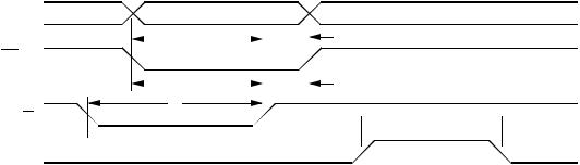
BIT 0–7
|
|
|
tDS |
|
|
tDH |
|
|
|
|
|
|
|||
HBE OR |
|||||||
|
|||||||
LBE |
|
||||||
|
|
|
|
|
|
||
|
|
|
tBES |
|
tBEH |
||
|
|
|
|
||||
|
|
|
|
|
|||
tCS
CS
 tLH
tLH 
 tLW
tLW 
LDAC
Figure 1a. AD660 Byte Load Timing
–4– |
REV. A |
Loading...