


AD650SD
Table of contents
 Loading...
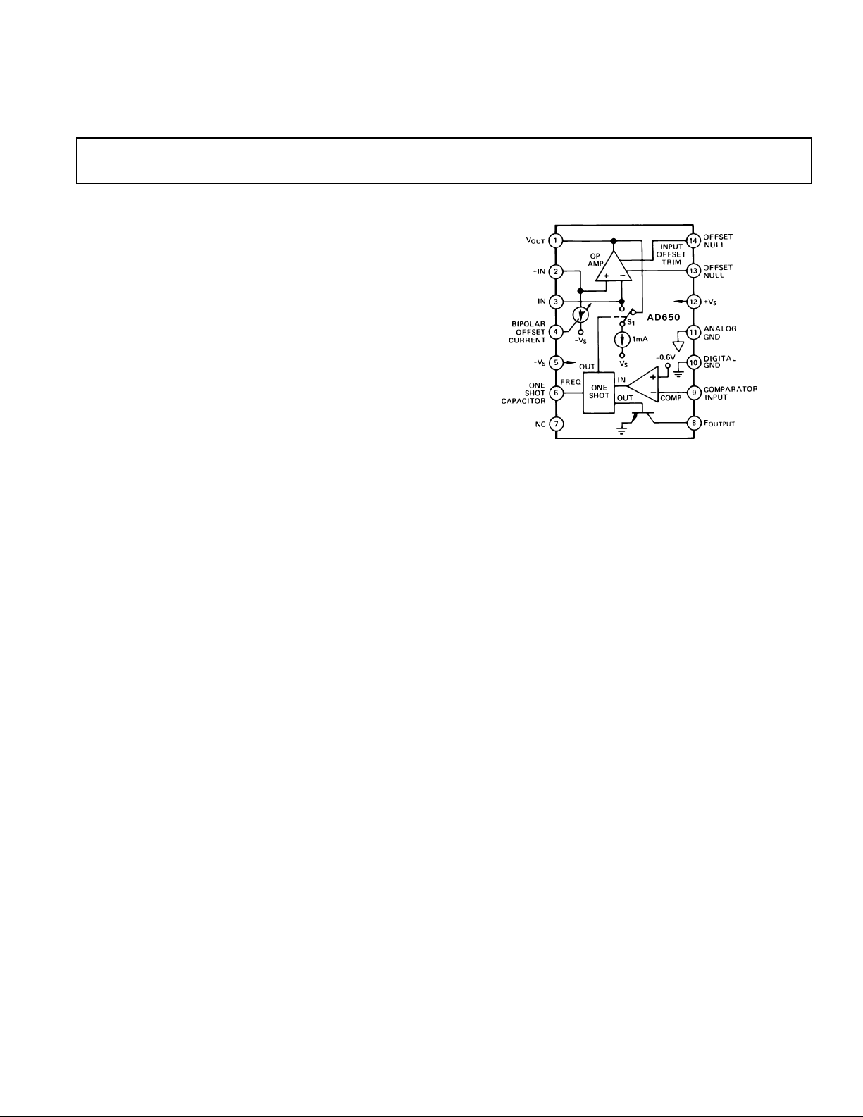
Voltage-to-Frequency and
a
FEATURES
V/F Conversion to 1 MHz
Reliable Monolithic Construction
Very Low Nonlinearity
0.002% typ at 10 kHz
0.005% typ at 100 kHz
0.07% typ at 1 MHz
Input Offset Trimmable to Zero
CMOS or TTL Compatible
Unipolar, Bipolar, or Differential V/F
V/F or F/V Conversion
Available in Surface Mount
MIL-STD-883 Compliant Versions Available
PRODUCT DESCRIPTION
The AD650 V/F/V (voltage-to-frequency or frequency-to-voltage
converter) provides a combination of high frequency operation
and low nonlinearity previously unavailable in monolithic form.
The inherent monotonicity of the V/F transfer function makes
the AD650 useful as a high-resolution analog-to-digital converter.
A flexible input configuration allows a wide variety of input voltage and current formats to be used, and an open-collector output
with separate digital ground allows simple interfacing to either
standard logic families or opto-couplers.
The linearity error of the AD650 is typically 20 ppm (0.002%
of full scale) and 50 ppm (0.005%) maximum at 10 kHz full
scale. This corresponds to approximately 14-bit linearity in an
analog-to-digital converter circuit. Higher full-scale frequencies
or longer count intervals can be used for higher resolution conversions. The AD650 has a useful dynamic range of six decades
allowing extremely high resolution measurements. Even at 1 MHz
full scale, linearity is guaranteed less than 1000 ppm (0.1%) on
the AD650KN, BD, and SD grades.
In addition to analog-to-digital conversion, the AD650 can be used
in isolated analog signal transmission applications, phased lockedloop circuits, and precision stepper motor speed controllers. In
the F/V mode, the AD650 can be used in precision tachometer
and FM demodulator circuits.
The input signal range and full-scale output frequency are userprogrammable with two external capacitors and one resistor.
Input offset voltage can be trimmed to zero with an external
potentiometer.
REV. C
Information furnished by Analog Devices is believed to be accurate and
reliable. However, no responsibility is assumed by Analog Devices for its
use, nor for any infringements of patents or other rights of third parties
which may result from its use. No license is granted by implication or
otherwise under any patent or patent rights of Analog Devices.
Frequency-to-Voltage Converter
AD650
PIN CONFIGURATION
The AD650JN and AD650KN are offered in a plastic 14-lead
DIP package. The AD650JP is available in a 20-lead plastic
leaded chip carrier (PLCC). Both plastic packaged versions of the
AD650 are specified for the commercial (0°C to +70°C) temperature range. For industrial temperature range (–25°C to +85°C)
applications, the AD650AD and AD650BD are offered in a
ceramic package. The AD650SD is specified for the full –55°C
to +125°C extended temperature range.
PRODUCT HIGHLIGHTS
1. In addition to very high linearity, the AD650 can operate at
full-scale output frequency up to 1 MHz. The combination of
these two features makes the AD650 an inexpensive solution
for applications requiring high resolution monotonic A/D
conversion.
2. The AD650 has a very versatile architecture that can be configured to accommodate bipolar, unipolar, or differential
input voltages, or unipolar input currents.
3. TTL or CMOS compatibility is achieved using an open
collector frequency output. The pull-up resistor can be
connected to voltages up to +30 V, or +15 V or +5 V for
conventional CMOS or TTL logic levels.
4. The same components used for V/F conversion can also be
used for F/V conversion by adding a simple logic biasing network and reconfiguring the AD650.
5. The AD650 provides separate analog and digital grounds.
This feature allows prevention of ground loops in real-world
applications.
6. The AD650 is available in versions compliant with MILSTD-883. Refer to the Analog Devices Military Products
Databook or current AD650/883B data sheet for detailed
specifications.
One Technology Way, P.O. Box 9106, Norwood, MA 02062-9106, U.S.A.
Tel: 781/329-4700 World Wide Web Site: http://www.analog.com
Fax: 781/326-8703 © Analog Devices, Inc., 2000

AD650–SPECIFICATIONS
(@ +25ⴗC, with VS = ⴞ15 V, unless otherwise noted)
AD650J/AD650A AD650K/AD650B AD650S
Model Min Typ Max Min Typ Max Min Typ Max Units
DYNAMIC PERFORMANCE
Full-Scale Frequency Range 1 1 1 MHz
Nonlinearity
Nonlinearity
Nonlinearity
Nonlinearity
Full-Scale Calibration Error
Full-Scale Calibration Error
vs. Supply
1
f
= 10 kHz 0.002 0.005 0.002 0.005 0.002 0.005 %
MAX
1
f
= 100 kHz 0.005 0.02 0.005 0.02 0.005 0.02 %
MAX
1
f
= 500 kHz 0.02 0.05 0.02 0.05 0.02 0.05 %
MAX
1
f
= 1 MHz 0.1 0.05 0.1 0.05 0.1 %
MAX
3
2
, 100 kHz ±5 ±5 ±5%
2
, 1 MHz ±10 ±10 ±10 %
–0.015 +0.015 –0.015 +0.015 –0.015 +0.015 % of FSR/V
vs. Temperaturc
A, B, and S Grades
at 10 kHz ±75 ±75 ±75 ppm/°C
at 100 kHz ±150 ±150 ±150 ppm/°C
J and K Grades
at 10 kHz ±75 ±75 ppm/°C
at 100 kHz ±150 ±150 ppm/°C
BIPOLAR OFFSET CURRENT
Activated by 1.24 kΩ Between Pins 4 and 5 0.45 0.5 0.55 0.45 0.5 0.55 0.45 0.5 0.55 mA
DYNAMIC RESPONSE
Maximum Settling Time for Full Scale
Step Input 1 Pulse of New Frequency Plus 1 µs 1 Pulse of New Frequency Plus 1 µs 1 Pulse of New Frequency Plus 1 µs
Overload Recovery Time
Step Input 1 Pulse of New Frequency Plus 1 µs 1 Pulse of New Frequency Plus 1 µs 1 Pulse of New Frequency Plus 1 µs
ANALOLG INPUT AMPLIFIER (V/F Conversion)
Current Input Range (Figure 1) 0 +0.6 0 +0.6 0 +0.6 mA
Voltage Input Range (Figure 5) –10 0 –10 0 –10 0 V
Differential Impedance 2 MΩ储10 pF 2 MΩ储10 pF 2 MΩ储10 pF
Common-Mode Impedance 1000 MΩ储10 pF 1000 MΩ储10 pF 1000 MΩ储10 pF
Input Bias Current
Noninverting Input 40 100 40 100 40 100 nA
Inverting Input ±8 ⴞ20 ±8 ⴞ20 ±8 ⴞ20 nA
Input Offset Voltage
(Trimmable to Zero) ⴞ4 ⴞ4 ⴞ4 mV
vs. Temperature (T
Safe Input Voltage ±V
MIN
to T
) ±30 ±30 ± 30 µ V/°C
MAX
S
±V
S
±V
S
C
COMPARATOR (F/V Conversion)
Logic “0” Level –V
Logic “1” Level 0 +V
Pulse Width Range
4
S
0.1 (0.3 × tOS) 0.1 (0.3 × tOS) 0.1 (0.3 × tOS) µs
–1 –V
0+V
S
S
–1 –V
0+V
S
S
+1 V
S
V
Input Impedance 250 250 250 kΩ
OPEN COLLECTOR OUTPUT (V/F Conversion)
Output Voltage in Logic “0”
I
≤ 8 mA, T
SINK
Output Leakage Current in Logic “1” 100 100 100 nA
Voltage Range
to T
MIN
MAX
5
0 +36 0 +36 0 +36 V
0.4 0.4 0.4 V
AMPLIFIER OUTPUT (F/V Conversion)
Voltage Range (1500 Ω min Load Resistance) 0 +10 0 +10 0 +10 V
Source Current (750 Ω max Load Resistance) 10 10 10 mA
Capacitive Load (Without Oscillation) 100 100 100 pF
POWER SUPPLY
Voltage, Rated Performance ± 9 ⴞ18 ±9 ⴞ18 ± 9 ⴞ18 V
Quiescent Current 88 8mA
TEMPERATURE RANGE
Rated Performance – N Package 0 +70 0 +70 °C
Rated Performance – D Package –25 +85 –25 +85 –55 +125 °C
NOTES
1
Nonlinearity is defined as deviation from a straight line from zero to full scale, expressed as a fraction of full scale.
2
Full-scale calibration error adjustable to zero.
3
Measured at full-scale output frequency of 100 kHz.
4
Refer to F/V conversion section of the text.
5
Referred to digital ground.
Specifications subject to change without notice.
Specifications shown in boldface are tested on all production units at final electrical test. Results from those test are used to calculate outgoing quality levels. All min and max
specifications are guaranteed, although only those shown in boldface are tested on all production units.
–2–
REV. C
AD650
ABSOLUTE MAXIMUM RATINGS
Total Supply Voltage . . . . . . . . . . . . . . . . . . . . . . . . . . . . . 36 V
Storage Temperature . . . . . . . . . . . . . . . . . . . –55°C to +150°C
Differential Input Voltage . . . . . . . . . . . . . . . . . . . . . . . ±10 V
Maximum Input Voltage . . . . . . . . . . . . . . . . . . . . . . . . . . ±V
Open Collector Output Voltage Above Digital GND . . . . . 36 V
Open Collector Output Current . . . . . . . . . . . . . . . . . . 50 mA
Amplifier Short Circuit to Ground . . . . . . . . . . . . . . Indefinite
Comparator Input Voltage . . . . . . . . . . . . . . . . . . . . . . . . . ± V
PIN CONFIGURATION
PIN
NO. D-14 N-14 P-20A
S
1V
OUT
2 +IN +IN V
3 –IN –IN +IN
S
4 BIPOLAR OFFSET BIPOLAR OFFSET –IN
CURRENT CURRENT
5–V
6 ONE SHOT ONE SHOT BIPOLAR OFFSET
7NC NC NC
8F
9 COMPARATOR COMPARATOR ONE SHOT
10 DIGITAL GND DIGITAL GND NC
11 ANALOG GND ANALOG GND NC
12 +V
13 OFFSET NULL OFFSET NULL COMPARATOR
14 OFFSET NULL OFFSET NULL DIGITAL GND
15 NC
16 ANALOG GND
17 NC
18 +V
19 OFFSET NULL
20 OFFSET NULL
S
CAPACITOR CAPACITOR CURRENT
OUTPUT
INPUT INPUT CAPACITOR
S
V
OUT
–V
S
F
OUTPUT
+V
S
NC
OUT
NC
–V
F
OUTPUT
INPUT
S
S
ORDERING GUIDE
Gain
Tempco Specified
ppm/ ⴗC 1 MHz Temperature Package Package
Model 100 kHz Linearity Range ⴗC Description Option
AD650JN 150 typ 0.1% typ 0 to +70 Plastic DIP N-14
AD650KN 150 typ 0.1% max 0 to +70 Plastic DIP N-14
AD650JP 150 typ 0.1% typ 0 to +70 Plastic Leaded Chip Carrier (PLCC) P-20A
AD650AD 150 max 0.1% typ –25 to +85 Ceramic DIP D-14
AD650BD 150 max 0.1% max –25 to +85 Ceramic DIP D-14
AD650SD 150 max 0.1% max –55 to +125 Ceramic DIP D-14
REV. C
–3–
AD650
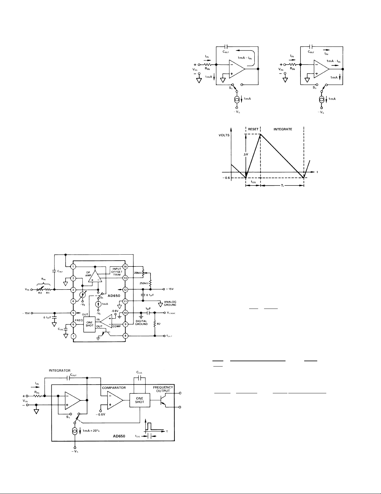
CIRCUIT OPERATION
UNIPOLAR CONFIGURATION
The AD650 is a charge balance voltage-to-frequency converter. In
the connection diagram shown in Figure 1, or the block diagram
of Figure 2a, the input signal is converted into an equivalent current by the input resistance R
by an internal feedback current delivered in short, timed bursts
from the switched 1 mA internal current source. These bursts of
current may be thought of as precisely defined packets of charge.
The required number of charge packets, each producing one
pulse of the output transistor, depends upon the amplitude of
the input signal. Since the number of charge packets delivered
per unit time is dependent on the input signal amplitude, a linear
voltage-to-frequency transformation will be accomplished. The
frequency output is furnished via an open collector transistor.
A more rigorous analysis demonstrates how the charge balance
voltage-to-frequency conversion takes place.
A block diagram of the device arranged as a V-to-F converter is
shown in Figure 2a. The unit is comprised of an input integrator, a current source and steering switch, a comparator and a
one-shot. When the output of the one-shot is low, the current
steering switch S
diverts all the current to the output of the op
1
amp; this is called the Integration Period. When the one-shot
has been triggered and its output is high, the switch S
all the current to the summing junction of the op amp; this is
called the Reset Period. The two different states are shown in
Figure 2 along with the various branch currents. It should be
noted that the output current from the op amp is the same for
either state, thus minimizing transients.
. This current is exactly balanced
IN
diverts
1
Figure 2b. Reset Mode Figure 2c. Integrate Mode
Figure 2d. Voltage Across C
INT
The positive input voltage develops a current (IIN = VIN/RIN)
which charges the integrator capacitor C
on C
, the output voltage of the integrator ramps downward
INT
. As charge builds up
INT
towards ground. When the integrator output voltage (Pin 1)
crosses the comparator threshold (–0.6 volt) the comparator
triggers the one shot, whose time period, t
the one shot capacitor C
OS
.
is determined by
OS
Specifically, the one shot time period is:
tOS= COS× 6.8 ×10³sec /F + 3. 0 ×10
–7 sec
(1)
The Reset Period is initiated as soon as the integrator output
voltage crosses the comparator threshold, and the integrator
ramps upward by an amount:
Figure 1. Connection Diagram for V/F Conversion,
Positive Input Voltage
Figure 2a. Block Diagram
dV
t
∆V =tOS•
OS
=
dt
1mA – I
()
C
INT
(2)
N
After the Reset Period has ended, the device starts another Integration Period, as shown in Figure 2, and starts ramping downward
again. The amount of time required to reach the comparator
threshold is given as:
t
∆
T
=
I
dV
OS/CINT
V
=
dt
(1 mA – IIN)
I
N/CINT
= t
OS
1 mA
–1
I
IN
The output frequency is now given as:
f
=
OUT
t
OS
Note that C
=
I
I
IN
tOS×1 mA
= 0.15
F•Hz
A
, the integration capacitor has no effect on the
1
+ T
INT
VIN/R
COS+ 4.4 ×10
IN
–11
(4)
F
transfer relation, but merely determines the amplitude of the
sawtooth signal out of the integrator.
One Shot Timing
A key part of the preceding analysis is the one shot time period
that was given in equation (1). This time period can be broken
down into approximately 300 ns of propagation delay, and a second time segment dependent linearly on timing capacitor C
OS
When the one shot is triggered, a voltage switch that holds Pin 6
–4–
REV. C
(3)
.
Loading...