


 Loading...
a |
4-Channel, 104 MSPS Digital |
|
Transmit Signal Processor (TSP) |
||
|
|
|
|
|
AD6623 |
|
|
|
FEATURES
Pin Compatible to the AD6622 18-Bit Parallel Digital IF Output Real or Interleaved Complex
18-Bit Bidirectional Parallel Digital IF Input/Output Allows Cascade of Chips for Additional Channels Clipped or Wrapped Over Range
Two’s Complement or Offset Binary Output
Four Independent Digital Transmitters in Single Package RAM Coefficient Filter (RCF)
Programmable IF and Modulation for Each Channel Programmable Interpolating RAM Coefficient Filter p/4-DQPSK Differential Phase Encoder
3p/8-PSK Linear Encoder 8-PSK Linear Encoder
Programmable GMSK Look-Up Table
Programmable QPSK Look-Up Table All-Pass Phase Equalizer Programmable Fine Scaler Programmable Power Ramp Unit
High Speed CIC Interpolating Filter
Digital Resampling for Noninteger Interpolation Rates NCO Frequency Translation
Spurious Performance Better than –100 dBc Separate 3-Wire Serial Data Input for Each Channel
Bidirectional Serial Clocks and Frames Microprocessor Control
2.5 V CMOS Core, 3.3 V Outputs, 5 V Inputs JTAG Boundary Scan
APPLICATIONS
Cellular/PCS Base Stations
Micro/Pico Cell Base Stations
Wireless Local Loop Base Stations
Multicarrier, Multimode Digital Transmit
GSM, EDGE, IS136, PHS, IS95, TDS CDMA, UMTS,
CDMA2000
Phased Array Beam Forming Antennas
Software Defined Radio
Tuning Resolution Better than 0.025 Hz
Real or Complex Outputs
FUNCTIONAL BLOCK DIAGRAM
NCO = NUMERICALLY CONTROLLED
OSCILLATOR/TUNER
SDINA |
|
|
|
|
|
|
|
|
|
|
|
|
|
|
I |
|
|
I |
|
|
|
I |
|
|
|
I |
|
|
|
|
||||||
|
|
|
|
|
|
|
|
DATA |
RAM |
SCALER |
|
CIC5 |
|
RCIC2 |
|
|
CHAN A |
|||||||||||||||||||
|
|
|
|
|
|
|
|
|
|
|
|
|
||||||||||||||||||||||||
|
|
|
|
|
|
|
|
|
|
|
|
|
|
|
|
|
|
|
|
|
|
|
||||||||||||||
SDFIA |
|
|
|
|
SPORT |
|
|
|
COEFFICIENT |
Q |
|
|
AND |
Q |
|
|
Q |
|
|
Q |
|
NCO |
|
|
||||||||||||
|
|
|
|
|
|
|
|
|
|
FILTER |
|
|
FILTER |
|
|
|
||||||||||||||||||||
SDFOA |
|
|
|
|
|
|
|
FILTER |
|
|
|
|
POWER |
|
|
|
|
|
|
|
|
|
|
|||||||||||||
|
|
|
|
|
|
|
|
|
|
|
|
|
|
|
|
|
|
|
|
|
|
|
|
|
|
|
|
|
|
|
||||||
|
|
|
|
|
|
|
|
|
|
|
|
|
|
|
|
|
|
RAMP |
|
|
|
|
|
|
|
|
|
|
|
|
|
|
|
|
||
|
|
|
|
|
|
|
|
|
|
|
|
|
|
|
|
|
|
|
|
|
|
|
|
|
|
|
|
|
|
|
|
|
|
|||
SCLKA |
|
|
|
|
|
|
|
|
|
|
|
|
|
|
|
|
|
|
|
|
|
|
|
|
|
|
|
|
|
|
|
|
|
|
|
|
|
|
|
|
|
|
|
|
|
|
|
|
|
|
|
|
|
|
|
|
|
|
|
|
|
|
|
|
|
|
|
|
|
|
|
|
|
|
|
|
|
|
|
|
|
|
|
|
|
|
|
|
|
|
|
|
|
|
|
|
|
|
|
|
|
|
|
|
|
|
|
|
|
|
SDINB |
|
|
|
|
|
|
|
|
|
|
|
|
|
|
I |
|
|
I |
|
|
|
I |
|
|
|
I |
|
|
|
|
||||||
|
|
|
|
|
|
|
|
DATA |
RAM |
SCALER |
|
CIC5 |
|
RCIC2 |
|
|
CHAN B |
|||||||||||||||||||
|
|
|
|
|
|
|
|
|
|
|
|
|
||||||||||||||||||||||||
SDFIB |
|
|
|
|
SPORT |
COEFFICIENT |
|
|
|
|
|
|
|
|
|
|
|
|
|
|
||||||||||||||||
|
|
|
|
|
|
|
Q |
AND |
Q |
|
Q |
|
Q |
NCO |
|
|
||||||||||||||||||||
|
|
|
|
|
|
FILTER |
|
FILTER |
|
|
||||||||||||||||||||||||||
|
|
|
|
|
|
|
||||||||||||||||||||||||||||||
SDFOB |
|
|
|
|
|
|
|
|
|
|
|
FILTER |
|
|
|
|
POWER |
|
|
|
|
|
|
|
|
|
|
|
||||||||
|
|
|
|
|
|
|
|
|
|
|
|
|
|
|
|
|
|
|
|
|
|
|
|
|
|
|
|
|
|
|
||||||
|
|
|
|
|
|
|
|
|
|
|
|
|
|
|
|
|
|
RAMP |
|
|
|
|
|
|
|
|
|
|
|
|
|
|
|
|
||
SCLKB |
|
|
|
|
|
|
|
|
|
|
|
|
|
|
|
|
|
|
|
|
|
|
|
|
|
|
|
|
|
|
|
|
|
|
|
|
|
|
|
|
|
|
|
|
|
|
|
|
|
|
|
|
|
|
|
|
|
|
|
|
|
|
|
|
|
|
|
|
|
|
|
|
|
|
|
|
|
|
|
|
|
|
|
|
|
|
|
|
|
|
|
|
|
|
|
|
|
|
|
|
|
|
|
|
|
|
|
|
|
|
SDINC |
|
|
|
|
|
|
|
|
|
|
|
|
|
|
I |
|
|
I |
|
|
|
I |
|
|
|
I |
|
|
|
|
||||||
|
|
|
|
|
|
|
|
|
DATA |
RAM |
|
|
|
|
SCALER |
|
|
|
CIC5 |
|
|
|
RCIC2 |
|
|
|
|
CHAN C |
||||||||
SDFIC |
|
|
|
|
SPORT |
|
|
|
COEFFICIENT |
Q |
|
|
|
AND |
Q |
|
|
Q |
|
|
Q |
|
NCO |
|
|
|||||||||||
|
|
|
|
|
|
|
|
|
FILTER |
|
|
FILTER |
|
|
|
|||||||||||||||||||||
SDFOC |
|
|
|
|
FILTER |
|
|
|
|
POWER |
|
|
|
|
|
|
|
|
|
|
|
|||||||||||||||
|
|
|
|
|
|
|
|
|
|
|
|
|
|
|
|
|
|
RAMP |
|
|
|
|
|
|
|
|
|
|
|
|
|
|
|
|
||
|
|
|
|
|
|
|
|
|
|
|
|
|
|
|
|
|
|
|
|
|
|
|
|
|
|
|
|
|
|
|
|
|
|
|||
SCLKC |
|
|
|
|
|
|
|
|
|
|
|
|
|
|
|
|
|
|
|
|
|
|
|
|
|
|
|
|
|
|
|
|
|
|
|
|
|
|
|
|
|
|
|
|
|
|
|
|
|
|
|
|
|
|
|
|
|
|
|
|
|
|
|
|
|
|
|
|
|
|
|
|
|
|
|
|
|
|
|
|
|
|
|
|
|
|
|
|
|
|
|
|
|
|
|
|
|
|
|
|
|
|
|
|
|
|
|
|
|
|
SDIND |
|
|
|
|
|
|
|
|
|
|
|
|
|
|
I |
|
|
|
I |
|
|
|
|
I |
|
|
|
|
I |
|
|
|
|
|
||
|
|
|
|
|
|
|
|
DATA |
RAM |
SCALER |
|
CIC5 |
|
RCIC2 |
|
|
CHAN D |
|||||||||||||||||||
|
|
|
|
|
|
|
|
|
|
|
|
|
||||||||||||||||||||||||
SDFID |
|
|
|
|
SP |
ORT |
|
|
|
COEFFICIENT |
Q |
AND |
Q |
|
Q |
|
Q |
NCO |
|
|
||||||||||||||||
|
|
|
|
|
|
|
FILTER |
|
FILTER |
|
|
|||||||||||||||||||||||||
SDFOD |
|
|
|
|
|
|
|
|
FILTER |
|
|
|
|
POWER |
|
|
|
|
|
|
|
|
|
|
|
|||||||||||
|
|
|
|
|
|
|
|
|
|
|
|
|
|
|
|
|
|
|
|
|
|
|
|
|
|
|
|
|
|
|
||||||
|
|
|
|
|
|
|
|
|
|
|
|
|
|
|
|
|
|
RAMP |
|
|
|
|
|
|
|
|
|
|
|
|
|
|
|
|
||
|
|
|
|
|
|
|
|
|
|
|
|
|
|
|
|
|
|
|
|
|
|
|
|
|
|
|
|
|
|
|
|
|
|
|||
SCLKD |
|
|
|
|
|
|
|
|
|
|
|
|
|
|
|
|
|
|
|
|
|
|
|
|
|
|
|
|
|
|
|
|
|
|
|
|
|
|
|
|
|
|
|
|
|
|
|
|
|
|
|
|
|
|
|
|
|
|
|
|
|
|
|
|
|
|
|
|
|
|
|
|
|
|
|
|
|
|
|
|
|
|
|
|
|
|
|
|
|
|
|
|
|
|
|
|
|
|
|
|
|
|
|
|
|
|
|
|
|
|
|
|
|
|
|
|
|
|
|
|
|
|
|
|
|
|
|
|
|
|
|
|
|
|
|
|
|
|
|
|
|
|
|
|
|
||
|
|
|
|
|
|
|
|
|
|
|
JTAG |
|
|
|
|
|
|
|
|
|
|
|
MICROPORT |
|
|
|
|
|
|
|||||||
|
|
|
|
|
|
|
|
|
|
|
|
|
|
|
|
|
|
|
|
|
|
|
|
|
|
|
|
|
|
|
|
|
|
|
|
|
|
|
|
|
|
|
|
|
|
|
|
|
|
|
|
|
|
|
|
|
|
|
|
|
|
|
|
|
|
|
|
|
|
|
|
|
|
|
|
|
|
|
|
|
|
|
|
|
|
|
|
|
|
|
|
|
|
|
|
|
|
|
|
|
|
|
|
|
|
|
|
|
|
|
|
|
|
|
|
|
|
|
|
|
|
|
|
|
|
|
|
|
|
|
|
|
|
|
|
|
|
|
|
|
|
|
|
|
|
|
|
|
|
|
|
|
|
|
|
|
|
|
|
|
|
|
|
|
|
|
|
|
|
|
|
|
|
|
|
|
|
|
|
|
|
|
|
|
 QIN
QIN
IN [17–0]
SYNC
4
SUMMATION
 OEN
OEN

 QOUT
QOUT
OUT [17:0]
TDL TDO TMS TCK TRST |
D[7:0] DS DTACK RW MODE A[2:0] CS |
CLK RESET |
REV. 0
Information furnished by Analog Devices is believed to be accurate and reliable. However, no responsibility is assumed by Analog Devices for its use, nor for any infringements of patents or other rights of third parties that may result from its use. No license is granted by implication or otherwise under any patent or patent rights of Analog Devices.
One Technology Way, P.O. Box 9106, Norwood, MA 02062-9106, U.S.A.
Tel: 781/329-4700 |
www.analog.com |
Fax: 781/326-8703 |
© Analog Devices, Inc., 2002 |

AD6623
TABLE OF CONTENTS
FEATURES . . . . . . . . . . . . . . . . . . . . . . . . . . . . . . . . . . . . . . . . . . . . . . . 1 APPLICATIONS . . . . . . . . . . . . . . . . . . . . . . . . . . . . . . . . . . . . . . . . . . . 1 FUNCTIONAL BLOCK DIAGRAM . . . . . . . . . . . . . . . . . . . . . . . . . . . 1 PRODUCT DESCRIPTION . . . . . . . . . . . . . . . . . . . . . . . . . . . . . . . . . . 3 FUNCTIONAL OVERVIEW . . . . . . . . . . . . . . . . . . . . . . . . . . . . . . . . . . 3 RECOMMENDED OPERATING CONDITIONS . . . . . . . . . . . . . . . . 4 ELECTRICAL CHARACTERISTICS . . . . . . . . . . . . . . . . . . . . . . . . . . 4
LOGIC INPUTS (5 V TOLERANT) . . . . . . . . . . . . . . . . . . . . . . . . . 4 LOGIC OUTPUTS . . . . . . . . . . . . . . . . . . . . . . . . . . . . . . . . . . . . . . . 4 IDD SUPPLY CURRENT . . . . . . . . . . . . . . . . . . . . . . . . . . . . . . . . . . 4 POWER DISSIPATION . . . . . . . . . . . . . . . . . . . . . . . . . . . . . . . . . . . 4 GENERAL TIMING CHARACTERISTICS . . . . . . . . . . . . . . . . . . . . . 5 MICROPROCESSOR PORT TIMING CHARACTERISTICS . . . . . . . . 6 MICROPROCESSOR PORT, MODE INM (MODE = 0) . . . . . . . . . 6 MICROPROCESSOR PORT, MOTOROLA (MODE = 1) . . . . . . . . 6 TIMING DIAGRAMS . . . . . . . . . . . . . . . . . . . . . . . . . . . . . . . . . . . . . 7–9 ABSOLUTE MAXIMUM RATINGS . . . . . . . . . . . . . . . . . . . . . . . . . . 10 THERMAL CHARACTERISTICS . . . . . . . . . . . . . . . . . . . . . . . . . . . . 10 EXPLANATION OF TEST LEVELS . . . . . . . . . . . . . . . . . . . . . . . . . . 10 ORDERING GUIDE . . . . . . . . . . . . . . . . . . . . . . . . . . . . . . . . . . . . . . . 10 ESD SENSITIVITY . . . . . . . . . . . . . . . . . . . . . . . . . . . . . . . . . . . . . . . . 10 PIN CONFIGURATION – 128-Lead MQFP . . . . . . . . . . . . . . . . . . . . 11 128 PIN FUNCTION DESCRIPTION . . . . . . . . . . . . . . . . . . . . . . . 12 PIN CONFIGURATION – 196-Lead BGA . . . . . . . . . . . . . . . . . . . . . . 13 196 PIN FUNCTION DESCRIPTION . . . . . . . . . . . . . . . . . . . . . . . 14 POWER SUPPLY . . . . . . . . . . . . . . . . . . . . . . . . . . . . . . . . . . . . . . . 14 INPUTS . . . . . . . . . . . . . . . . . . . . . . . . . . . . . . . . . . . . . . . . . . . . . . . 14 CONTROL . . . . . . . . . . . . . . . . . . . . . . . . . . . . . . . . . . . . . . . . . . . . . 14 MICROPORT CONTROL . . . . . . . . . . . . . . . . . . . . . . . . . . . . . . . . 14 OUTPUTS . . . . . . . . . . . . . . . . . . . . . . . . . . . . . . . . . . . . . . . . . . . . . 14 JTAG AND BIST . . . . . . . . . . . . . . . . . . . . . . . . . . . . . . . . . . . . . . . . 14 SERIAL DATA PORT . . . . . . . . . . . . . . . . . . . . . . . . . . . . . . . . . . . . . . 15 Serial Master Mode (SCS = 0) . . . . . . . . . . . . . . . . . . . . . . . . . . . . . . 15 Serial Slave Mode (SCS = 1) . . . . . . . . . . . . . . . . . . . . . . . . . . . . . . . 15 Self-Framing Mode . . . . . . . . . . . . . . . . . . . . . . . . . . . . . . . . . . . . . . . 15 External Framing Mode . . . . . . . . . . . . . . . . . . . . . . . . . . . . . . . . . . . 15 Serial Port Cascade Configuration . . . . . . . . . . . . . . . . . . . . . . . . . . . 15 Serial Data Format . . . . . . . . . . . . . . . . . . . . . . . . . . . . . . . . . . . . . . . 15 PROGRAMMABLE RAM COEFFICIENT FILTER (RCF) . . . . . . . . . 16 OVERVIEW OF THE RCF BLOCKS . . . . . . . . . . . . . . . . . . . . . . . . 16 INTERPOLATING FIR FILTER . . . . . . . . . . . . . . . . . . . . . . . . . . . 17 RCF CONTROL REGISTERS . . . . . . . . . . . . . . . . . . . . . . . . . . . . . 19 PSK MODULATOR . . . . . . . . . . . . . . . . . . . . . . . . . . . . . . . . . . . . . 19/4-DQSPK MODULATION . . . . . . . . . . . . . . . . . . . . . . . . . . . . 20 8-PSK MODULATION . . . . . . . . . . . . . . . . . . . . . . . . . . . . . . . . . 20 3 /8-8-PSK MODULATION . . . . . . . . . . . . . . . . . . . . . . . . . . . . 20 MSK Look-Up Table . . . . . . . . . . . . . . . . . . . . . . . . . . . . . . . . . . . . . 21 GMSK Look-Up Table . . . . . . . . . . . . . . . . . . . . . . . . . . . . . . . . . . . . 21 QPSK Look-Up Table . . . . . . . . . . . . . . . . . . . . . . . . . . . . . . . . . . . . 21 PHASE EQUALIZER . . . . . . . . . . . . . . . . . . . . . . . . . . . . . . . . . . . . 21 SCALE AND RAMP . . . . . . . . . . . . . . . . . . . . . . . . . . . . . . . . . . . . . 21 FINE SCALING . . . . . . . . . . . . . . . . . . . . . . . . . . . . . . . . . . . . . . . . . . . 21 RCF POWER RAMPING . . . . . . . . . . . . . . . . . . . . . . . . . . . . . . . . . . . 21
CASCADED INTERGRATOR COMB (CIC)
INTERPOLATING FILTERS . . . . . . . . . . . . . . . . . . . . . . . . . . . . . . . . 21 CIC Scaling . . . . . . . . . . . . . . . . . . . . . . . . . . . . . . . . . . . . . . . . . . . . . 22 CIC5 . . . . . . . . . . . . . . . . . . . . . . . . . . . . . . . . . . . . . . . . . . . . . . . . . . 22 rCIC2 . . . . . . . . . . . . . . . . . . . . . . . . . . . . . . . . . . . . . . . . . . . . . . . . . 23
NUMERICALLY CONTROLLED
OSCILLATOR/TUNER (NCO) . . . . . . . . . . . . . . . . . . . . . . . . . . . . . . . . 24 Phase Dither . . . . . . . . . . . . . . . . . . . . . . . . . . . . . . . . . . . . . . . . . . . . 25 Amplitude Dither . . . . . . . . . . . . . . . . . . . . . . . . . . . . . . . . . . . . . . . . 25 Phase Offset . . . . . . . . . . . . . . . . . . . . . . . . . . . . . . . . . . . . . . . . . . . . 25 NCO Frequency Update and Phase Offset Update
Hold-Off Counters . . . . . . . . . . . . . . . . . . . . . . . . . . . . . . . . . . . . . . . 25 NCO Control Scale . . . . . . . . . . . . . . . . . . . . . . . . . . . . . . . . . . . . . . . 25 SUMMATION BLOCK . . . . . . . . . . . . . . . . . . . . . . . . . . . . . . . . . . . . . 25 SYNCHRONIZATION . . . . . . . . . . . . . . . . . . . . . . . . . . . . . . . . . . . . . 26 Start . . . . . . . . . . . . . . . . . . . . . . . . . . . . . . . . . . . . . . . . . . . . . . . . . . 26
Start with No Sync . . . . . . . . . . . . . . . . . . . . . . . . . . . . . . . . . . . . . . . |
26 |
Start with Soft Sync . . . . . . . . . . . . . . . . . . . . . . . . . . . . . . . . . . . . . . |
27 |
Start with Pin Sync . . . . . . . . . . . . . . . . . . . . . . . . . . . . . . . . . . . . . . . |
27 |
Hop with Soft Sync . . . . . . . . . . . . . . . . . . . . . . . . . . . . . . . . . . . . . . . |
27 |
Hop with Pin Sync . . . . . . . . . . . . . . . . . . . . . . . . . . . . . . . . . . . . . . . |
27 |
Beam with Soft Sync . . . . . . . . . . . . . . . . . . . . . . . . . . . . . . . . . . . . . . |
28 |
Beam with Pin Sync . . . . . . . . . . . . . . . . . . . . . . . . . . . . . . . . . . . . . . |
28 |
JTAG INTERFACE . . . . . . . . . . . . . . . . . . . . . . . . . . . . . . . . . . . . . . . . |
28 |
SCALING . . . . . . . . . . . . . . . . . . . . . . . . . . . . . . . . . . . . . . . . . . . . . . . . |
28 |
Multicarrier Scaling . . . . . . . . . . . . . . . . . . . . . . . . . . . . . . . . . . . . . . |
28 |
Single Carrier Scaling . . . . . . . . . . . . . . . . . . . . . . . . . . . . . . . . . . . . . |
29 |
MICROPORT INTERFACE . . . . . . . . . . . . . . . . . . . . . . . . . . . . . . . . . |
29 |
MicroPort Control . . . . . . . . . . . . . . . . . . . . . . . . . . . . . . . . . . . . . . |
29 |
EXTERNAL MEMORY MAP . . . . . . . . . . . . . . . . . . . . . . . . . . . . . . . . |
29 |
Intel Nonmultiplexed Mode (INM) . . . . . . . . . . . . . . . . . . . . . . . . . . |
30 |
Motorola Nonmultiplexed Mode (MNM) . . . . . . . . . . . . . . . . . . . . . |
30 |
External Address 7 Upper Address Register (UAR) . . . . . . . . . . . . . . |
30 |
External Address 6 Lower Address Register (LAR) . . . . . . . . . . . . . . |
30 |
External Address 5 Sync . . . . . . . . . . . . . . . . . . . . . . . . . . . . . . . . . . . |
30 |
External Address 4 Sleep . . . . . . . . . . . . . . . . . . . . . . . . . . . . . . . . . . |
31 |
External Address 3:0 (Data Bytes) . . . . . . . . . . . . . . . . . . . . . . . . . . . |
31 |
INTERNAL CONTROL REGISTERS AND ON-CHIP RAM . . . . . . . . . |
31 |
AD6623 and AD6622 Compatibility |
|
Common Function Registers (not associated |
|
with a particular channel) . . . . . . . . . . . . . . . . . . . . . . . . . . . . . . . . |
31 |
Channel Function Registers (0x1XX = Ch. A, |
|
0x2XX = Ch. B, 0x3XX = Ch. C, 0x4XX = Ch. D) . . . . . . . . . . . |
31 |
(0x000) Summation Mode Control . . . . . . . . . . . . . . . . . . . . . . . . . . |
33 |
(0x001) Sync Mode Control . . . . . . . . . . . . . . . . . . . . . . . . . . . . . . . . |
33 |
(0x002) BIST Counter . . . . . . . . . . . . . . . . . . . . . . . . . . . . . . . . . . . . |
33 |
(0x003) BIST Result . . . . . . . . . . . . . . . . . . . . . . . . . . . . . . . . . . . . . . |
33 |
Channel Function Registers . . . . . . . . . . . . . . . . . . . . . . . . . . . . . . . . |
34 |
(0xn00) Start Update Hold-Off Counter . . . . . . . . . . . . . . . . . . . . . . |
34 |
(0xn01) NCO Control . . . . . . . . . . . . . . . . . . . . . . . . . . . . . . . . . . . . |
34 |
(0xn02) NCO Frequency . . . . . . . . . . . . . . . . . . . . . . . . . . . . . . . . . . |
34 |
(0xn03) NCO Frequency Update Hold-Off Counter . . . . . . . . . . . . . |
34 |
(0xn04) NCO Phase Offset . . . . . . . . . . . . . . . . . . . . . . . . . . . . . . . . . |
34 |
(0xn05) NCO Phase Offset Update Hold-Off Counter . . . . . . . . . . . . |
34 |
(0xn06) CIC Scale . . . . . . . . . . . . . . . . . . . . . . . . . . . . . . . . . . . . . . . |
34 |
(0xn07) CIC2 Decimation – 1 (MCIC2 – 1) . . . . . . . . . . . . . . . . . . . . . |
34 |
(0xn08) CIC2 Interpolation – 1 (LCIC2 – 1) . . . . . . . . . . . . . . . . . . . . |
34 |
(0xn09) CIC5 Interpolation . . . . . . . . . . . . . . . . . . . . . . . . . . . . . . . . |
34 |
(0xn0A) Number of RCF Coefficients – 1 . . . . . . . . . . . . . . . . . . . . . |
34 |
(0xn0B) RCF Coefficient Offset . . . . . . . . . . . . . . . . . . . . . . . . . . . . . |
34 |
(0xn0C) Channel Mode Control 1 . . . . . . . . . . . . . . . . . . . . . . . . . . . |
34 |
(0xn0D) Channel Mode Control 2 . . . . . . . . . . . . . . . . . . . . . . . . . . . |
35 |
(0xn0E) Fine Scale Factor . . . . . . . . . . . . . . . . . . . . . . . . . . . . . . . . . |
35 |
(0xn0F) RCF Time Slot Hold-Off Counter . . . . . . . . . . . . . . . . . . . . |
35 |
(0xn10–0xn11) RCF Phase Equalizer Coefficients . . . . . . . . . . . . . . . |
35 |
(0xn12–0xn15) FIR-PSK Magnitudes . . . . . . . . . . . . . . . . . . . . . . . . |
35 |
(0xn16) Serial Port Setup . . . . . . . . . . . . . . . . . . . . . . . . . . . . . . . . . . |
35 |
(0xn17) Power Ramp Length 0 . . . . . . . . . . . . . . . . . . . . . . . . . . . . . . |
35 |
(0xn18) Power Ramp Length 1 . . . . . . . . . . . . . . . . . . . . . . . . . . . . . . |
35 |
(0xn19) Power Ramp Rest Time . . . . . . . . . . . . . . . . . . . . . . . . . . . . . |
35 |
(0xn20–0xn1F) Unused . . . . . . . . . . . . . . . . . . . . . . . . . . . . . . . . . . . |
35 |
(0xn20–0xn3F) Data Memory . . . . . . . . . . . . . . . . . . . . . . . . . . . . . . |
35 |
(0xn40–0xn17F) Power Ramp Coefficient Memory . . . . . . . . . . . . . . |
35 |
Pseudocode . . . . . . . . . . . . . . . . . . . . . . . . . . . . . . . . . . . . . . . . . . . . . |
35 |
Write Pseudocode . . . . . . . . . . . . . . . . . . . . . . . . . . . . . . . . . . . . . . |
35 |
Read Pseudocode . . . . . . . . . . . . . . . . . . . . . . . . . . . . . . . . . . . . . . |
36 |
APPLICATIONS . . . . . . . . . . . . . . . . . . . . . . . . . . . . . . . . . . . . . . . . . . |
36 |
USING THE AD6623 TO PROCESS UMTS CARRIERS . . . . . . . . |
36 |
DIGITAL-TO-ANALOG CONVERTER (DAC) SELECTION . . . . . . . |
36 |
MULTIPLE TSP OPERATION . . . . . . . . . . . . . . . . . . . . . . . . . . . . |
36 |
Determining the Number of TSPs to Use . . . . . . . . . . . . . . . . . . . . |
36 |
Programming Mulitple TSPs . . . . . . . . . . . . . . . . . . . . . . . . . . . . . |
37 |
Driving Multiple TSP Serial Ports . . . . . . . . . . . . . . . . . . . . . . . . . |
37 |
THERMAL MANAGEMENT . . . . . . . . . . . . . . . . . . . . . . . . . . . . . . |
38 |
PACKAGE OUTLINE DIMENSIONS . . . . . . . . . . . . . . . . . . . . . . . . . |
39 |
–2– |
REV. 0 |

AD6623
PRODUCT DESCRIPTION
The AD6623 is a 4-channel Transmit Signal Processor (TSP) that creates high bandwidth data for Transmit Digital-to-Analog Converters (TxDACs) from baseband data provided by a Digital Signal Processor (DSP). Modern TxDACs have achieved sufficiently high sampling rates, analog bandwidth, and dynamic range to create the first Intermediate Frequency (IF) directly. The AD6623 synthesizes multicarrier and multistandard digital signals to drive these TxDACs. The RAM-based architecture allows easy reconfiguration for multimode applications. Modulation, pulseshaping and anti-imaging filters, static equalization, and tuning functions are combined in a single, cost-effective device. Digital IF signal processing provides repeatable manufacturing, higher accuracy, and more flexibility than comparable high dynamic range analog designs.
The AD6623 has four identical digital TSPs complete with synchronization circuitry and cascadable wideband channel summation. AD6623 is pin compatible to AD6622 and can operate in AD6622compatible control register mode.
The AD6623 utilizes a 3.3 V I/O power supply and a 2.5 V core power supply. All I/O pins are 5 V tolerant. All control registers and coefficient values are programmed through a generic microprocessor interface. Intel and Motorola microprocessor bus modes are supported. All inputs and outputs are LVCMOS compatible.
FUNCTIONAL OVERVIEW
Each TSP has five cascaded signal processing elements: a programmable interpolating RAM Coefficient Filter (RCF), a programmable Scale and Power Ramp, a programmable fifth order Cascaded Integrator Comb (CIC5) interpolating filter, a flexible second order Resampling Cascaded Integrator Comb filter (rCIC2), and a Numerically Controlled Oscillator/Tuner (NCO).
The outputs of the four TSPs are summed and scaled on-chip. In multicarrier wideband transmitters, a bidirectional bus allows the Parallel (wideband) IF Input/Output to drive a second DAC. In this operational mode two AD6623 channels drive one DAC and the other two AD6623 channels drive a second DAC. Multiple AD6623s may be combined by driving the INOUT[17:0] of the succeeding with the OUT[17:0] of the preceding chip. The
INOUT[17:0] can alternatively be masked off by software to allow preceding AD6623’s outputs to be ignored.
Each channel accepts input data from independent serial ports that may be connected directly to the serial port of Digital Signal Processor (DSP) chips.
The RCF implements any one of the following functions: Interpolating Finite Impulse Response (FIR) filter, /4-DQPSK modulator, 8-PSK modulator, or 3 /8-8-PSK modulator, GMSK modulator, and QPSK modulator. Each AD6623 channel can be dynamically switched between the GMSK modulation mode and the 3 /8-8-PSK modulation mode in order to support the GSM/EDGE standard. The RCF also implements an Allpass Phase Equalizer (APE) which meets the requirements of IS-95-A/B standard (CDMA transmission).
The programmable Scale and Power Ramp block allows power ramping on a time-slot basis as specified for some air-interface standards (e.g., GSM, EDGE). A fine scaling unit at the programmable FIR filter output allows an easy signal amplitude level adjustment on time slot basis.
The CIC5 provides integer rate interpolation from 1 to 32 and coarse anti-image filtering. The rCIC2 provides fractional rate interpolation from 1 to 4096 in steps of 1/512. The wide range of interpolation factors in each CIC filter stage and a highly flexible resampler incorporated into rCIC2 makes the AD6623 useful for creating both narrowband and wideband carriers in a high-speed sample stream.
The high resolution 32-bit NCO allows flexibility in frequency planning and supports both digital and analog air interface standards. The high speed NCO tunes the interpolated complex signal from the rCIC2 to an IF channel. The result may be real or complex. Multicarrier phase synchronization pins and phase offset registers allow intelligent management of the relative phase of independent RF channels. This capability supports the requirements for phased array antenna architectures and management of the wideband peak/power ratio to minimize clipping at the DAC.
The wideband Output Ports can deliver real or complex data. Complex words are interleaved into real (I) and imaginary (Q) parts at half the master clock rate.
REV. 0 |
–3– |
AD6623
RECOMMENDED OPERATING CONDITIONS
|
Test |
|
AD6623 |
|
|
Parameter |
Level |
Min |
Typ |
Max |
Unit |
|
|
|
|
|
|
VDD |
IV |
2.25 |
2.5 |
2.75 |
V |
VDDIO |
IV |
3.0 |
3.3 |
3.6 |
V |
TAMBIENT |
IV |
–40 |
+25 |
+70 |
°C |
ELECTRICAL CHARACTERISTICS
Parameter (Conditions) |
Temp |
Test Level |
Min |
Typ |
Max |
Unit |
|
|
|
|
|
|
|
LOGIC INPUTS (5 V TOLERANT) |
|
|
|
|
|
|
Logic Compatibility |
Full |
|
|
3.3 V CMOS |
|
|
Logic “1” Voltage |
Full |
IV |
2.0 |
|
5.0 |
V |
Logic “0” Voltage |
Full |
IV |
–0.3 |
|
+0.8 |
V |
Logic “1” Current |
Full |
IV |
|
1 |
10 |
A |
Logic “0” Current |
Full |
IV |
|
0 |
10 |
A |
Input Capacitance |
25°C |
V |
|
4 |
|
pF |
LOGIC OUTPUTS |
|
|
|
|
|
|
Logic Compatibility |
Full |
|
|
3.3 V CMOS/TTL |
|
|
Logic “1” Voltage (IOH = 0.25 mA) |
Full |
IV |
2.0 |
VDD – 0.2 |
|
V |
Logic “0” Voltage (IOL = 0.25 mA) |
Full |
IV |
|
0.2 |
0.4 |
V |
IDD SUPPLY CURRENT |
|
|
|
|
|
|
CLK = 104 MHz, VDD = 2.75 V* |
Full |
IV |
|
422 |
TBD* |
mA |
CLK = 104 MHz, VDDIO = 3.6 V* |
Full |
IV |
|
193 |
|
mA |
GSM Example: CORE |
|
V |
|
232 |
|
mA |
I/O |
|
|
|
56 |
|
mA |
IS-136 Example: CORE |
|
V |
|
207 |
|
mA |
I/O |
|
|
|
55 |
|
mA |
WBCDMA Example |
|
V |
|
Tbd |
|
mA |
Sleep Mode |
Full |
IV |
|
Tbd |
TBD |
mA |
|
|
|
|
|
|
|
POWER DISSIPATION |
|
|
|
|
|
|
GSM Example |
|
V |
|
740 |
|
mW |
IS-136 Example |
|
V |
|
700 |
|
mW |
WBCDMA Example |
|
V |
|
Tbd |
|
mW |
Sleep Mode |
Full |
IV |
|
Tbd |
TBD |
mW |
|
|
|
|
|
|
|
*This specification denotes an absolute maximum supply current for the device. The conditions include all channels active, minimum interpolation in both CIC stages, and maximum switching of input data. In an actual application the power will be less.
See the Thermal Management section of the data sheet for further details.
–4– |
REV. 0 |
|
|
|
|
|
|
|
AD6623 |
|
GENERAL TIMING CHARACTERISTICS1, 2 |
|
|
|
|
|
|
|
|
|
|
|
Test |
|
AD6623AS |
|
|
|
Parameter (Conditions) |
Temp |
Level |
Min |
Typ |
Max |
Unit |
||
|
|
|
|
|
|
|
|
|
CLK Timing Requirements: |
|
|
|
|
|
|
|
|
tCLK |
CLK Period |
Full |
I |
9.6 |
|
|
ns |
|
tCLKL |
CLK Width Low |
Full |
IV |
3 |
0.5 × tCLK |
|
ns |
|
tCLKH |
CLK Width High |
Full |
IV |
3 |
|
ns |
||
RESET Timing Requirement: |
|
|
|
|
|
|
|
|
tRESL |
RESET Width Low |
Full |
I |
30.0 |
|
|
ns |
|
Input Data Timing Requirements: |
|
|
|
|
|
|
|
|
tSI |
INOUT[17:0], QIN to ↑CLK Setup Time |
Full |
IV |
1 |
|
|
ns |
|
tHI |
INOUT[17:0], QIN to ↑CLK Hold Time |
Full |
IV |
2 |
|
|
ns |
|
Output Data Timing Characteristics: |
|
|
|
|
|
|
|
|
tDO |
↑CLK to OUT[17:0], INOUT[17:0], |
|
|
|
|
|
|
|
|
QOUT Output Delay Time |
Full |
IV |
2 |
|
6 |
ns |
|
tDZO |
OEN HIGH to OUT[17:0] Active |
Full |
IV |
3 |
|
7.5 |
ns |
|
SYNC Timing Requirements: |
|
|
|
|
|
|
|
|
tSS |
SYNC(0, 1, 2, 3) to ↑CLK Setup Time |
Full |
IV |
1 |
|
|
ns |
|
tHS |
SYNC(0, 1, 2, 3) to ↑CLK Hold Time |
Full |
IV |
2 |
|
|
ns |
|
Master Mode Serial Port Timing Requirements (SCS = 0): |
|
|
|
|
|
|
|
|
Switching Characteristics3 |
|
|
|
|
|
|
|
|
tDSCLK1 |
↑CLK to ↑SCLK Delay (divide by 1) |
Full |
IV |
4 |
|
10.5 |
ns |
|
tDSCLKH |
↑CLK to ↑SCLK Delay (for any other divisor) |
Full |
IV |
5 |
|
13 |
ns |
|
tDSCLKL |
↑CLK to ↓SCLK Delay |
|
|
|
|
|
|
|
|
(divide by 2 or even number) |
Full |
IV |
3.5 |
|
9 |
ns |
|
tDSCLKLL |
↓CLK to ↓SCLK Delay |
|
|
|
|
|
|
|
|
(divide by 3 or odd number) |
Full |
IV |
4 |
|
10 |
ns |
|
|
Channel is Self-Framing |
|
|
|
|
|
|
|
tSSDI0 |
SDIN to ↑SCLK Setup Time |
Full |
IV |
1.7 |
|
|
ns |
|
tHSDI0 |
SDIN to ↑SCLK Hold Time |
Full |
IV |
0 |
|
|
ns |
|
tDSFO0A |
↑SCLK to SDFO Delay |
Full |
IV |
0.5 |
|
3.5 |
ns |
|
|
Channel is External-Framing |
|
|
|
|
|
|
|
tSSFI0 |
SDFI to ↑SCLK Setup Time |
Full |
IV |
2 |
|
|
ns |
|
tHSFI0 |
SDFI to ↑SCLK Hold Time |
Full |
IV |
0 |
|
|
ns |
|
tSSDI0 |
SDIN to ↑SCLK Setup Time |
Full |
IV |
2 |
|
|
ns |
|
tHSDI0 |
SDIN to ↑SCLK Hold Time |
Full |
IV |
0 |
|
|
ns |
|
tDSFO0B |
↑SCLK to SDFO Delay |
Full |
IV |
0.5 |
|
3 |
ns |
|
Slave Mode Serial Port Timing Requirements (SCS = 1): |
|
|
|
|
|
|
|
|
Switching Characteristics3 |
|
|
|
|
|
|
|
|
tSCLK |
SCLK Period |
Full |
IV |
|
2 tCLK |
|
ns |
|
tSCLKL |
SCLK Low Time |
Full |
IV |
3.5 |
|
|
ns |
|
tSCLKH |
SCLK High Time |
Full |
IV |
3.5 |
|
|
ns |
|
|
Channel is Self-Framing |
|
|
|
|
|
|
|
tSSDH |
SDIN to ↑SCLK Setup Time |
Full |
IV |
1 |
|
|
ns |
|
tHSDH |
SDIN to ↑SCLK Hold Time |
Full |
IV |
2.5 |
|
|
ns |
|
tDSFO1 |
↑SCLK to SDFO Delay |
Full |
IV |
4 |
|
10 |
ns |
|
|
Channel is External-Framing |
|
|
|
|
|
|
|
tSSFI1 |
SDFI to ↑ SCLK Setup Time |
Full |
IV |
2 |
|
|
ns |
|
tHSFI1 |
SDFI to ↑SCLK Hold Time |
Full |
IV |
1 |
|
|
ns |
|
tSSDI1 |
SDIN to ↑SCLK Setup Time |
Full |
IV |
1 |
|
|
ns |
|
tHSDI1 |
SDIN to ↑SCLK Hold Time |
Full |
IV |
2.5 |
|
|
ns |
|
tDSFO1 |
↓SCLK to SDFO Delay |
Full |
IV |
10 |
|
|
ns |
|
NOTES
1All Timing Specifications valid over VDD range of 2.375 V to 2.675 V and VDDIO range of 3.0 V to 3.6 V. 2CLOAD = 40 pF on all outputs (unless otherwise specified).
3The timing parameters for SCLK, SDIN, SDFI, SDFO, and SYNC apply to all four channels (A, B, C, and D).
Specifications subject to change without notice.
REV. 0 |
–5– |
AD6623
MICROPROCESSOR PORT TIMING CHARACTERISTICS1, 2
|
|
|
Test |
|
AD6623AS |
|
|||
Parameter (Conditions) |
Temp |
Level |
|
Min |
Typ |
Max |
Unit |
||
|
|
|
|
|
|
|
|
|
|
MICROPROCESSOR PORT, MODE INM (MODE = 0) |
|
|
|
|
|
|
|
|
|
|
|
|
|
|
|
|
|
|
|
MODE INM Write Timing: |
|
|
|
|
|
|
|
|
|
tSC |
Control3 to ↑CLK Setup Time |
Full |
IV |
4.5 |
|
|
|
ns |
|
tHC |
Control3 to ↑CLK Hold Time |
Full |
IV |
2.0 |
|
|
|
ns |
|
tHWR |
WR(RW) to RDY(DTACK) Hold Time |
Full |
IV |
8.0 |
|
|
|
ns |
|
tSAM |
Address/Data to WR(RW) Setup Time |
Full |
IV |
3.0 |
|
|
|
ns |
|
tHAM |
Address/Data to RDY(DTACK) Hold Time |
Full |
IV |
2.0 |
|
|
|
ns |
|
tDRDY |
WR(RW) to RDY(DTACK) Delay |
Full |
IV |
4.0 |
|
|
|
ns |
|
tACC |
WR(RW) to RDY(DTACK) High Delay |
Full |
IV |
4 × tCLK |
5 × tCLK |
|
9 × tCLK |
ns |
|
MODE INM Read Timing: |
|
|
|
|
|
|
|
|
|
tSC |
Control3 to ↑CLK Setup Time |
Full |
IV |
4.5 |
|
|
|
ns |
|
tHC |
Control3 to ↑CLK Hold Time |
Full |
IV |
2.0 |
|
|
|
ns |
|
tSAM |
Address to RD(DS) Setup Time |
Full |
IV |
3.0 |
|
|
|
ns |
|
tHAM |
Address to Data Hold Time |
Full |
IV |
2.0 |
|
|
|
ns |
|
tZOZ |
Data Three-State Delay |
Full |
IV |
|
|
|
|
ns |
|
tDD |
RDY(DTACK) to Data Delay |
Full |
IV |
|
|
|
|
ns |
|
tDRDY |
RD(DS) to RDY(DTACK) Delay |
Full |
IV |
4.0 |
|
|
|
ns |
|
tACC |
RD(DS) to RDY(DTACK) High Delay |
Full |
IV |
8 × tCLK |
10 × tCLK |
13 × tCLK |
ns |
||
MICROPROCESSOR PORT, MOTOROLA (MODE = 1) |
|
|
|
|
|
|
|
|
|
|
|
|
|
|
|
|
|
|
|
MODE MNM Write Timing: |
|
|
|
|
|
|
|
|
|
tSC |
Control3 to ↑CLK Setup Time |
Full |
IV |
4.5 |
|
|
|
ns |
|
tHC |
Control3 to ↑CLK Hold Time |
Full |
IV |
2.0 |
|
|
|
ns |
|
tHDS |
DS(RD) to DTACK(RDY) Hold Time |
Full |
IV |
8.0 |
|
|
|
ns |
|
tHRW |
RW(WR) to DTACK(RDY) Hold Time |
Full |
IV |
8.0 |
|
|
|
ns |
|
tSAM |
Address/Data to RW(WR) Setup Time |
Full |
IV |
3.0 |
|
|
|
ns |
|
tHAM |
Address/Data to RW(WR) Hold Time |
Full |
IV |
2.0 |
|
|
|
ns |
|
tDDTACK |
DS(RD) to DTACK(RDY) Delay |
|
|
|
4 × tCLK |
5 × tCLK |
|
9 × tCLK |
ns |
tACC |
RW(WR) to DTACK(RDY) Low Delay |
Full |
IV |
|
ns |
||||
MODE MNM Read Timing: |
|
|
|
|
|
|
|
|
|
tSC |
Control3 to ↑CLK Setup Time |
Full |
IV |
4.0 |
|
|
|
ns |
|
tHC |
Control3 to ↑CLK Hold Time |
Full |
IV |
2.0 |
|
|
|
ns |
|
tHDS |
DS(RD) to DTACK(RDY) Hold Time |
Full |
IV |
8.0 |
|
|
|
ns |
|
tSAM |
Address to DS(RD) Setup Time |
Full |
IV |
3.0 |
|
|
|
ns |
|
tHAM |
Address to Data Hold Time |
Full |
IV |
2.0 |
|
|
|
ns |
|
tZD |
Data Three-State Delay |
Full |
IV |
|
|
|
|
ns |
|
tDD |
DTACK(RDY) to Data Delay |
Full |
IV |
|
|
|
|
ns |
|
tDDTACK |
DS(RD) to DTACK(RDY) Delay |
Full |
IV |
8 × tCLK |
10 × tCLK |
13 × tCLK |
ns |
||
tACC |
DS(RD) to DTACK(RDY) Low Delay |
Full |
IV |
ns |
|||||
NOTES
1All Timing Specifications valid over VDD range of 2.375 V to 2.675 V and VDDIO range of 3.0 V to 3.6 V. 2CLOAD = 40 pF on all outputs (unless otherwise specified).
3Specification pertains to control signals: RW, (WR), DS, (RD), CS.
Specifications subject to change without notice.
–6– |
REV. 0 |

AD6623
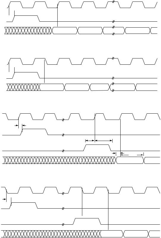
TIMING DIAGRAMS
|
|
|
|
|
tCLK |
|
|
|
|
|
|
|
|
|
|
|
||
|
|
|
|
|
|
|||||||||||||
CLK |
|
tCLKH |
|
tCLKL |
|
|
|
|
RESET |
|
|
|
|
|
||||
|
|
|
|
|
|
|
|
|
|
|
|
|||||||
|
|
|
|
|
|
|
|
|
|
|
|
|||||||
INOUT[17:0] |
|
|
|
|
|
|
|
|
|
|
|
|
||||||
|
|
|
|
|
|
|
|
|
|
|
||||||||
|
|
|
|
|
|
|
|
|
|
|||||||||
|
|
|
|
|||||||||||||||
|
|
|
|
|
|
|
|
|
|
|
|
|
|
|
|
|||
OUT[17:0] |
|
|
|
|
|
|
|
|
|
|
|
|
|
|
|
tRESL |
||
QOUT |
|
tDO |
|
|
|
|
|
|
|
|
|
|
|
|
|
|||
|
|
|
|
|
|
|
|
|
|
|
|
|
|
|||||
|
tZO |
|
|
|
|
|
|
tZO |
|
|
|
|
|
|
|
|
||
|
|
|
|
|
|
|
|
|
|
|
|
|
|
|
||||
|
|
|
|
|
|
|
|
|
|
|
|
|
|
|
|
|
||
|
|
|
|
|
|
|
|
|
||||||||||
|
|
|
|
|
|
|
|
|
|
|
|
|
|
|
|
|
|
|
|
|
|
|
|
|
|
|
|
|
|
|
|
|
|
|
|
|
|
OEN
Figure 1. Parallel Output Switching Characteristics Figure 4. RESET Timing Requirements
CLK

 tSI
tSI 

 tHI
tHI
INOUT[17:0]
QIN
Figure 2. Wideband Input Timing
CLK

 tSS
tSS 

 tHS
tHS 

SYNC
CLK
 tDSCLKH
tSCLKH
SCLK
tSCLKL
Figure 5. SCLK Switching Characteristics (Divide by 1)
CLK
tDSCLKH |
tDSCLKL |
|
SCLK
Figure 3. SYNC Timing Inputs |
Figure 6. SCLK Switching Characteristic (Divide by 2 or |
|
EVEN Integer) |
CLK
 tDSCLKH
 tDSCLKLL
SCLK
Figure 7. SCLK Switching Characteristic (Divide by 3 or ODD Integer)
REV. 0 |
–7– |
AD6623
SCLK
 tDSFO0A
SDFO
tSSDI0

 tHSDI0
SDIN |
DATAn |
Figure 8. Serial Port Timing, Master Mode (SCS = 0), Channel is Self-Framing
SCLK
 tDSFO1
SDFO
tSSDI1 


 tHSDI1
SDIN |
DATAn |
Figure 9. Serial Port Timing, Slave Mode (SCS = 1), Channel is Self-Framing
nCLKs |
|
|
SCLK |
|
|
tDSFO0B |
|
|
SDFO |
|
|
tSSFI0 |
|
tHSFI0 |
SDFI |
|
|
|
tSSDI0 |
tHSDI0 |
|
|
|
SDIN |
|
DATAn |
Figure 10. Serial Port Timing, Master Mode (SCS = 0), Channel is External-Framing
nCLKs
SCLK
 tDSFO1
SDFO
tSSFI1 


 tHSFI1
SDFI
tSSDI1 


 tHSDI1
SDIN |
DATAn |
Figure 11. Serial Port Timing, Slave Mode (SCS = 1), Channel is External-Framing
–8– |
REV. 0 |

AD6623
TIMING DIAGRAMS—INM MICROPORT MODE
CLK
RD (DS)
 tHC
tHC
tSC |
tHWR |
WR (RW)
CS

 tSAM tHAM
A[2:0] |
VALID ADDRESS |
tSAM tHAM
D[7:0]
VALID DATA
tDRDY
RDY (DTACK)
tACC
NOTES
1.tACC ACCESS TIME DEPENDS ON THE ADDRESS ACCESSED. ACCESS TIME IS MEASURED FROM FE OF WR TO THE RE OF RDY.
2.tACC REQUIRES A MAXIMUM 9 CLK PERIODS.
Figure 12. INM Microport Write Timing Requirements
CLK
tSC |
tHC |
RD (DS)
WR (RW)
CS
tSAM |
|
|
|
A[2:0] |
VALID ADDRESS |
|
|
t |
tDD |
tHAM |
t |
ZD |
|
|
ZD |
D[7:0] |
|
VALID DATA |
|
 tDRDY
tDRDY
RDY (DTACK)
tACC
NOTES
1.tACC ACCESS TIME DEPENDS ON THE ADDRESS ACCESSED. ACCESS TIME IS MEASURED FROM FE OF WR TO THE RE OF RDY.
2.tACC REQUIRES A MAXIMUM OF 13 CLK PERIODS AND APPLIES TO A[2:0] = 7, 6, 5, 3, 2, 1
Figure 13. INM Microport Read Timing Requirements
TIMING DIAGRAMS—MNM MICROPORT MODE
CLK |
|
|
tSC |
tHC |
|
tHDS |
||
|
||
DS (RD) |
|
|
|
tHRW |
RW (WR)
CS |
|
|
|
tSAM |
tHAM |
A[2:0] |
VALID ADDRESS |
|
|
t |
tHAM |
|
SAM |
|
D[7:0] |
VALID DATA |
|
tDDTACK
DTACK
(RDY)
tACC
NOTES
1.tACC ACCESS TIME DEPENDS ON THE ADDRESS ACCESSED. ACCESS TIME IS MEASURED FROM FE OF DS TO THE FE OF DTACK.
2.tACC REQUIRES A MAXIMUM 9 CLK PERIODS.
Figure 14. MNM Microport Write Timing Requirements
CLK
 tHC
tHC
tSC tHDS
DS (RD)
RW (WR)
CS |
|
|
|
tSAM |
|
|
|
A[2:0] |
|
VALID ADDRESS |
|
t |
tDD |
t |
t |
ZD |
|
HAM |
ZD |
D[7:0] |
|
VALID DATA |
|
|
|
tDDTACK |
|
DTACK
(RDY)
tACC
NOTES
1.tACC ACCESS TIME DEPENDS ON THE ADDRESS ACCESSED. ACCESS TIME IS MEASURED FROM FE OF DS TO THE FE OF DTACK.
2.tACC REQUIRES A MAXIMUM 13 CLK PERIODS.
Figure 15. Motorola Microport Read Timing Requirements
REV. 0 |
–9– |

AD6623
ABSOLUTE MAXIMUM RATINGS*
Supply Voltage . . . . . . . . . . . . . . . . . . . . . . . . . . . . . . . . . 3.6 V Input Voltage . . . . . . . . . . . . . . –0.3 V to +5 V (5 V Tolerant) Output Voltage Swing . . . . . . . . . . –0.3 V to VDDIO + 0.3 V Load Capacitance . . . . . . . . . . . . . . . . . . . . . . . . . . . . 200 pF Junction Temperature Under Bias . . . . . . . . . . . . . . . . . 125°C Storage Temperature Range . . . . . . . . . . . . –65°C to +150°C Lead Temperature (5 sec) . . . . . . . . . . . . . . . . . . . . . . . 280°C
*Stresses greater than those listed above may cause permanent damage to the device. These are stress ratings only; functional operation of the devices at these or any other conditions greater than those indicated in the operational sections of this specification is not implied. Exposure to absolute maximum rating conditions for extended periods may affect device reliability.
THERMAL CHARACTERISTICS
128-Lead MQFP:
JA = 33°C/W, no airflow
JA = 27°C/W, 200 lfpm airflowJA = 24°C/W, 400 lfpm airflow
196-Lead BGA:
JA = 26.3°C/W, no airflow
JA = 22°C/W, 200 lfpm airflow
Thermal measurements made in the horizontal position on a 2-layer board.
EXPLANATION OF TEST LEVELS
I. 100% Production Tested
II. 100% Production Tested at 25°C, and Sample Tested at
Specified Temperatures
III. Sample Tested Only
IV. Parameter Guaranteed by Design and Analysis
V. Parameter is Typical Value Only
ORDERING GUIDE
Model |
Temperature Range |
Package Description |
Package Option |
|
|
|
|
AD6623AS |
–40°C to +70°C (Ambient) |
128-Lead MQFP (Metric Quad Flatpack) |
S-128A |
AD6623ABC |
–40°C to +85°C (Ambient) |
196-Lead BGA (Ball Grid Array) |
BC-196 |
AD6623S/PCB |
|
MQFP Evaluation Board with AD6623 and Software |
|
AD6623BC/PCB |
|
BGA Evaluation Board with AD6623 and Software |
|
|
|
|
|
CAUTION
ESD (electrostatic discharge) sensitive device. Electrostatic charges as high as 4000 V readily accumulate on the human body and test equipment and can discharge without detection. Although the AD6623 features proprietary ESD protection circuitry, permanent damage may occur on devices subjected to high-energy electrostatic discharges. Therefore, proper ESD precautions are recommended to avoid performance degradation or loss of functionality.
WARNING!
ESD SENSITIVE DEVICE
–10– |
REV. 0 |
|
|
|
|
|
|
|
|
|
|
|
|
|
|
|
|
|
|
|
|
|
|
|
|
|
|
|
|
|
|
|
|
|
|
|
|
|
|
|
|
|
|
|
|
AD6623 |
|
|
|
|
|
|
|
|
|
|
|
|
|
|
|
|
|
|
|
|
|
|
|
|
|
|
|
|
|
|
|
|
|
|
|
|
|
|
|
|
|
|
|
|
|
|
|
|
|
|
|
|
|
|
|
|
|
|
|
|
|
|
|
PIN CONFIGURATION |
|
|
|
|
|
|
|
|
|
|
|
|
|
|
|
|
||||||||||
|
|
|
|
|
|
|
|
|
|
|
|
|
|
|
|
|
|
|
|
128-Lead MQFP |
|
|
|
|
|
|
|
|
|
|
|
|
|
|
|
|
|
|||||||
|
|
|
GND |
|
TCK |
TRST |
GND |
GND |
INOUT0 |
GND |
GND |
INOUT1 |
INOUT2 |
INOUT3 |
INOUT4 |
VDDIO |
INOUT5 |
INOUT6 |
INOUT7 |
INOUT8 |
GND |
GND |
GND |
INOUT9 |
INOUT10 |
INOUT11 |
INOUT12 |
VDDIO |
INOUT13 |
INOUT14 |
INOUT15 |
INOUT16 |
SYNC3 |
GND |
INOUT17 |
QIN |
SYNC2 |
GND |
CLK |
VDD |
GND |
|
||
|
|
|
|
|
|
|
|
|
|
|
|
|
|
|
|
|
|
|
|
|
|
|
|
|
|
|
|
|
|
|
|
|
|
|
|
|
|
|
|
|
|
|
|
|
|
|
|
102 |
|
101 |
100 |
99 |
98 |
97 |
96 |
95 |
94 |
93 |
92 |
91 |
90 |
89 |
88 |
87 |
86 |
85 |
84 |
83 |
82 |
81 |
80 |
79 |
78 |
77 |
76 |
75 |
74 |
73 |
72 |
71 |
70 |
69 |
68 |
67 |
66 |
65 |
|
|
|
|
|
|
|
|
|
|
|
|
|
|
|
|
|
|
|
|
|
|
|
|
|
|
|
|
|
|
|
|
|
|
|
|
|
|
|
|
|
|
|
|
|
|
|
|
GND |
103 |
|
|
|
|
|
|
|
|
|
|
|
|
|
|
|
|
|
|
|
|
|
|
|
|
|
|
|
|
|
|
|
|
|
|
|
|
|
|
|
|
64 |
GND |
|
|
|
|
|
|
|
|
|
|
|
|
|
|
|
|
|
|
|
|
|
|
|
|
|
|
|
|
|
|
|
|
|
|
|
|
|
|
|
|
|
|
|
|
|
SYNC1 |
VDD |
104 |
|
|
|
|
|
|
|
|
|
|
|
|
|
|
|
|
|
|
|
|
|
|
|
|
|
|
|
|
|
|
|
|
|
|
|
|
|
|
|
|
63 |
||
|
|
|
|
|
|
|
|
|
|
|
|
|
|
|
|
|
|
|
|
|
|
|
|
|
|
|
|
|
|
|
|
|
|
|
|
|
|
|
|
|
|
|
|
SYNC0 |
SDFIA |
105 |
|
|
|
|
|
|
|
|
|
|
|
|
|
|
|
|
|
|
|
|
|
|
|
|
|
|
|
|
|
|
|
|
|
|
|
|
|
|
|
|
62 |
||
|
|
|
|
|
|
|
|
|
|
|
|
|
|
|
|
|
|
|
|
|
|
|
|
|
|
|
|
|
|
|
|
|
|
|
|
|
|
|
|
|
|
|
|
|
TMS |
106 |
|
|
|
|
|
|
|
|
|
|
|
|
|
|
|
|
|
|
|
|
|
|
|
|
|
|
|
|
|
|
|
|
|
|
|
|
|
|
|
|
61 |
RESET |
|
|
|
|
|
|
|
|
|
|
|
|
|
|
|
|
|
|
|
|
|
|
|
|
|
|
|
|
|
|
|
|
|
|
|
|
|
|
|
|
|
|
|
|
|
|
TDO |
107 |
|
|
|
|
|
|
|
|
|
|
|
|
|
|
|
|
|
|
|
|
|
|
|
|
|
|
|
|
|
|
|
|
|
|
|
|
|
|
|
|
60 |
CS |
|
|
|
|
|
|
|
|
|
|
|
|
|
|
|
|
|
|
|
|
|
|
|
|
|
|
|
|
|
|
|
|
|
|
|
|
|
|
|
|
|
|
|
|
|
VDD |
TDI |
108 |
|
|
|
|
|
|
|
|
|
|
|
|
|
|
|
|
|
|
|
|
|
|
|
|
|
|
|
|
|
|
|
|
|
|
|
|
|
|
|
|
59 |
||
|
|
|
|
|
|
|
|
|
|
|
|
|
|
|
|
|
|
|
|
|
|
|
|
|
|
|
|
|
|
|
|
|
|
|
|
|
|
|
|
|
|
|
|
A0 |
SCLKA |
109 |
|
|
|
|
|
|
|
|
|
|
|
|
|
|
|
|
|
|
|
|
|
|
|
|
|
|
|
|
|
|
|
|
|
|
|
|
|
|
|
|
58 |
||
|
|
|
|
|
|
|
|
|
|
|
|
|
|
|
|
|
|
|
|
|
|
|
|
|
|
|
|
|
|
|
|
|
|
|
|
|
|
|
|
|
|
|
|
A1 |
VDDIO |
110 |
|
|
|
|
|
|
|
|
|
|
|
|
|
|
|
|
|
|
|
|
|
|
|
|
|
|
|
|
|
|
|
|
|
|
|
|
|
|
|
|
57 |
||
|
|
|
|
|
|
|
|
|
|
|
|
|
|
|
|
|
|
|
|
|
|
|
|
|
|
|
|
|
|
|
|
|
|
|
|
|
|
|
|
|
|
|
|
A2 |
SDFOA |
111 |
|
|
|
|
|
|
|
|
|
|
|
|
|
|
|
|
|
|
|
|
|
|
|
|
|
|
|
|
|
|
|
|
|
|
|
|
|
|
|
|
56 |
||
|
|
|
|
|
|
|
|
|
|
|
|
|
|
|
|
|
|
|
|
|
|
|
|
|
|
|
|
|
|
|
|
|
|
|
|
|
|
|
|
|
|
|
|
MODE |
SDINA |
112 |
|
|
|
|
|
|
|
|
|
|
|
|
|
|
|
|
|
|
|
|
|
|
|
|
|
|
|
|
|
|
|
|
|
|
|
|
|
|
|
|
55 |
||
|
|
|
|
|
|
|
|
|
|
|
|
|
|
|
|
|
|
|
|
|
|
|
|
|
|
|
|
|
|
|
|
|
|
|
|
|
|
|
|
|
|
|
|
GND |
SCLKB |
113 |
|
|
|
|
|
|
|
|
|
|
|
|
|
|
|
|
|
|
|
|
|
|
|
|
|
|
|
|
|
|
|
|
|
|
|
|
|
|
|
|
54 |
||
|
|
|
|
|
|
|
|
|
|
|
|
|
|
|
|
|
|
|
|
|
|
|
|
|
|
|
|
|
|
|
|
|
|
|
|
|
|
|
|
|
|
|
|
GND |
SDFOB |
114 |
|
|
|
|
|
|
|
|
|
|
|
|
|
|
|
|
|
|
AD6623 |
|
|
|
|
|
|
|
|
|
|
|
|
|
|
|
|
|
|
53 |
|||||
|
|
|
|
|
|
|
|
|
|
|
|
|
|
|
|
|
|
|
|
|
|
|
|
|
|
|
|
|
|
|
|
|
|
|
|
|
|
|
|
GND |
||||
SDFIB |
115 |
|
|
|
|
|
|
|
|
|
|
|
|
|
|
|
|
|
|
|
|
|
|
|
|
|
|
|
|
|
|
|
|
|
|
|
|
52 |
||||||
|
|
|
|
|
|
|
|
|
|
|
|
|
|
|
|
|
|
|
|
|
TOP VIEW |
|
|
|
|
|
|
|
|
|
|
|
|
|
|
|
|
|
|
|
RW(WR) |
|||
GND |
116 |
|
|
|
|
|
|
|
|
|
|
|
|
|
|
|
|
|
|
|
|
|
|
|
|
|
|
|
|
|
|
|
|
|
|
|
|
51 |
||||||
|
|
|
|
|
|
|
|
|
|
|
|
|
|
|
|
|
|
|
|
|
(Not to Scale) |
|
|
|
|
|
|
|
|
|
|
|
|
|
|
|
|
|
|
|
DTACK(RDY) |
|||
SDFIC |
117 |
|
|
|
|
|
|
|
|
|
|
|
|
|
|
|
|
|
|
|
|
|
|
|
|
|
|
|
|
|
|
|
|
|
|
|
|
|
|
|
|
50 |
||
|
|
|
|
|
|
|
|
|
|
|
|
|
|
|
|
|
|
|
|
|
|
|
|
|
|
|
|
|
|
|
|
|
|
|
|
|
|
|
|
|
|
|
|
DS(RD) |
SDINB |
118 |
|
|
|
|
|
|
|
|
|
|
|
|
|
|
|
|
|
|
|
|
|
|
|
|
|
|
|
|
|
|
|
|
|
|
|
|
|
|
|
|
49 |
||
|
|
|
|
|
|
|
|
|
|
|
|
|
|
|
|
|
|
|
|
|
|
|
|
|
|
|
|
|
|
|
|
|
|
|
|
|
|
|
|
|
|
|
|
D0 |
SCLKC |
119 |
|
|
|
|
|
|
|
|
|
|
|
|
|
|
|
|
|
|
|
|
|
|
|
|
|
|
|
|
|
|
|
|
|
|
|
|
|
|
|
|
48 |
||
|
|
|
|
|
|
|
|
|
|
|
|
|
|
|
|
|
|
|
|
|
|
|
|
|
|
|
|
|
|
|
|
|
|
|
|
|
|
|
|
|
|
|
|
VDD |
SDFOC |
120 |
|
|
|
|
|
|
|
|
|
|
|
|
|
|
|
|
|
|
|
|
|
|
|
|
|
|
|
|
|
|
|
|
|
|
|
|
|
|
|
|
47 |
||
|
|
|
|
|
|
|
|
|
|
|
|
|
|
|
|
|
|
|
|
|
|
|
|
|
|
|
|
|
|
|
|
|
|
|
|
|
|
|
|
|
|
|
|
D1 |
SDINC |
121 |
|
|
|
|
|
|
|
|
|
|
|
|
|
|
|
|
|
|
|
|
|
|
|
|
|
|
|
|
|
|
|
|
|
|
|
|
|
|
|
|
46 |
||
|
|
|
|
|
|
|
|
|
|
|
|
|
|
|
|
|
|
|
|
|
|
|
|
|
|
|
|
|
|
|
|
|
|
|
|
|
|
|
|
|
|
|
|
D2 |
VDDIO |
122 |
|
|
|
|
|
|
|
|
|
|
|
|
|
|
|
|
|
|
|
|
|
|
|
|
|
|
|
|
|
|
|
|
|
|
|
|
|
|
|
|
45 |
||
|
|
|
|
|
|
|
|
|
|
|
|
|
|
|
|
|
|
|
|
|
|
|
|
|
|
|
|
|
|
|
|
|
|
|
|
|
|
|
|
|
|
|
|
D3 |
SCLKD |
123 |
|
|
|
|
|
|
|
|
|
|
|
|
|
|
|
|
|
|
|
|
|
|
|
|
|
|
|
|
|
|
|
|
|
|
|
|
|
|
|
|
44 |
||
|
|
|
|
|
|
|
|
|
|
|
|
|
|
|
|
|
|
|
|
|
|
|
|
|
|
|
|
|
|
|
|
|
|
|
|
|
|
|
|
|
|
|
|
D4 |
SDFOD |
124 |
|
|
|
|
|
|
|
|
|
|
|
|
|
|
|
|
|
|
|
|
|
|
|
|
|
|
|
|
|
|
|
|
|
|
|
|
|
|
|
|
43 |
||
|
|
|
|
|
|
|
|
|
|
|
|
|
|
|
|
|
|
|
|
|
|
|
|
|
|
|
|
|
|
|
|
|
|
|
|
|
|
|
|
|
|
|
|
GND |
SDIND |
125 |
|
|
|
|
|
|
|
|
|
|
|
|
|
|
|
|
|
|
|
|
|
|
|
|
|
|
|
|
|
|
|
|
|
|
|
|
|
|
|
|
42 |
||
|
|
|
|
|
|
|
|
|
|
|
|
|
|
|
|
|
|
|
|
|
|
|
|
|
|
|
|
|
|
|
|
|
|
|
|
|
|
|
|
|
|
|
|
VDDIO |
SDFID |
126 |
|
|
|
|
|
|
|
|
|
|
|
|
|
|
|
|
|
|
|
|
|
|
|
|
|
|
|
|
|
|
|
|
|
|
|
|
|
|
|
|
41 |
||
|
|
|
|
|
|
|
|
|
|
|
|
|
|
|
|
|
|
|
|
|
|
|
|
|
|
|
|
|
|
|
|
|
|
|
|
|
|
|
|
|
|
|
|
D5 |
VDD |
127 |
|
|
|
|
|
|
|
|
|
|
|
|
|
|
|
|
|
|
|
|
|
|
|
|
|
|
|
|
|
|
|
|
|
|
|
|
|
|
|
|
40 |
||
|
|
|
|
|
|
|
|
|
|
|
|
|
|
|
|
|
|
|
|
|
|
|
|
|
|
|
|
|
|
|
|
|
|
|
|
|
|
|
|
|
|
|
|
GND |
GND |
128 |
|
|
|
|
|
|
|
|
|
|
|
|
|
|
|
|
|
|
|
|
|
|
|
|
|
|
|
|
|
|
|
|
|
|
|
|
|
|
|
|
39 |
||
|
|
|
|
|
|
|
|
|
|
|
|
|
|
|
|
|
|
|
|
|
|
|
|
|
|
|
|
|
|
|
|
|
|
|
|
|
|
|
|
|
|
|
|
|
|
|
|
1 |
|
2 |
3 |
4 |
5 |
6 |
7 |
8 |
9 |
10 |
11 |
12 |
13 |
14 |
15 |
16 |
17 |
18 |
19 |
20 |
21 |
22 |
23 |
24 |
25 |
26 |
27 |
28 |
29 |
30 |
31 |
32 |
33 |
34 |
35 |
36 |
37 |
38 |
|
|
|
|
|
|
|
|
|
|
|
|
|
|
|
|
|
|
|
|
|
|
|
|
|
|
|
|
|
|
|
|
|
|
|
|
|
|
|
|
|
|
|
|
|
|
|
|
|
|
|
GND |
|
OEN |
GND |
GND |
GND |
OUT0 |
OUT1 |
OUT2 |
GND |
OUT3 |
OUT4 |
OUT5 |
OUT6 |
VDDIO |
OUT7 |
OUT8 |
OUT9 |
OUT10 |
GND |
GND |
GND |
OUT11 |
OUT12 |
OUT13 |
OUT14 |
VDDIO |
OUT15 |
OUT16 |
OUT17 |
QOUT |
GND |
GND |
D7 |
GND |
GND |
GND |
D6 |
GND |
|
||
REV. 0 |
–11– |
AD6623
128 PIN FUNCTION DESCRIPTIONS
Pin Number |
Mnemonic |
Type |
Description |
|
|
|
|
1, 3–5, 9, 19–21, 31, 32, 34–36, 38, 39, |
|
|
|
42, 52–54, 64–65, 68, 72, 83–85, 95, 96, |
|
|
|
98, 99, 102, 103, 116, 128 |
GND |
P |
Ground Connection |
2 |
OEN1 |
I |
Active High Output Enable Pin |
29, 28, 27, 25, 24, 23, 22, 18, 17, 16, 15, |
|
|
|
13, 12, 11, 10, 8, 7, 6 |
OUT[17:0] |
O/T |
Parallel Output Data |
47, 59, 66, 104, 127 |
VDD |
P |
2.5 V Supply |
14, 26, 41, 78, 90, 110, 122 |
VDDIO |
P |
3.3 V Supply |
30 |
QOUT |
O/T |
When HIGH indicates Q Output Data |
|
|
|
(Complex Output Mode) |
33, 37, 40, 43, 44, 45, 46, 48 |
D[7:0] |
I/O/T |
Bidirectional Microport Data |
49 |
DS (RD) |
I |
INM Mode: Read Signal, MNM Mode: Data Strobe Signal |
50 |
DTACK |
|
|
|
(RDY) |
O |
Acknowledgment of a Completed Transaction (Signals when |
|
|
|
P Port Is Ready for an Access) Open Drain, Must Be |
|
|
|
Pulled Up Externally |
51 |
RW (WR) |
I |
Active HIGH Read, Active Low Write |
55 |
MODE |
I |
Sets Microport Mode: MODE = 1, MNM Mode; MODE = 0, |
|
|
|
INM Mode |
56, 57, 58 |
A[2:0] |
I |
Microport Address Bus |
60 |
CS |
I |
Chip Select, Active low enable for P Access |
61 |
RESET2 |
I |
Active Low Reset Pin |
62 |
SYNC01 |
I |
SYNC Signal for Synchronizing Multiple AD6623s |
63 |
SYNC11 |
I |
SYNC Signal for Synchronizing Multiple AD6623s |
67 |
CLK1 |
I |
Input Clock |
69 |
SYNC21 |
I |
SYNC Signal for Synchronizing Multiple AD6623s |
70 |
QIN1 |
I |
When HIGH indicates Q input data (Complex Input Mode) |
71, 74–77, 79–82, 86–89, 91–94, 97 |
INOUT[17:0]1 |
I/O |
Wideband Input/Output Data (Allows Cascade of Multiple |
|
|
|
AD6623 Chips In a System) |
73 |
SYNC31 |
I |
SYNC Signal for Synchronizing Multiple AD6623s |
100 |
TRST2 |
I |
Test Reset Pin |
101 |
TCK1 |
I |
Test Clock Input |
105 |
SDFIA |
I |
Serial Data Frame Input—Channel A |
106 |
TMS2 |
I |
Test Mode Select |
107 |
TDO |
O |
Test Data Output |
108 |
TDI1 |
I |
Test Data Input |
109 |
SCLKA |
I/O |
Bidirectional Serial Clock—Channel A |
111 |
SDFOA |
O |
Serial Data Frame Sync Output—Channel A |
112 |
SDINA1 |
I |
Serial Data Input—Channel A |
113 |
SCLKB |
I/O |
Bidirectional Serial Clock—Channel B |
114 |
SDFOB |
O |
Serial Data Frame Sync Output—Channel B |
115 |
SDFIB |
I |
Serial Data Frame Input —Channel B |
117 |
SDFIC |
I |
Serial Data Frame Input—Channel C |
118 |
SDINB1 |
I |
Serial Data Input—Channel B |
119 |
SCLKC |
I/O |
Bidirectional Serial Clock—Channel C |
120 |
SDFOC |
O |
Serial Data Frame Sync Output—Channel C |
121 |
SDINC1 |
I |
Serial Data Input—Channel C |
123 |
SCLKD |
I/O |
Bidirectional Serial Clock—Channel D |
124 |
SDFOD |
O |
Serial Data Frame Sync Outpu—Channel D |
125 |
SDIND1 |
I |
Serial Data Input—Channel D |
126 |
SDFID |
I |
Serial Data Frame Input—Channel D |
|
|
|
|
NOTES
1Pins with a Pull-Down resistor of nominal 70 kΩ. 2Pins with a Pull-Up resistor of nominal 70 kΩ.
–12– |
REV. 0 |
Loading...