


AD652SQ
FUNCTIONAL BLOCK DIAGRAM
REV. B
Information furnished by Analog Devices is believed to be accurate and
reliable. However, no responsibility is assumed by Analog Devices for its
use, nor for any infringements of patents or other rights of third parties
which may result from its use. No license is granted by implication or
otherwise under any patent or patent rights of Analog Devices.
a
Monolithic Synchronous
Voltage-to-Frequency Converter
AD652
One Technology Way, P.O. Box 9106, Norwood, MA 02062-9106, U.S.A.
Tel: 781/329-4700 World Wide Web Site: http://www.analog.com
Fax: 781/326-8703 © Analog Devices, Inc., 2000
FEATURES
Full-Scale Frequency (Up to 2 MHz) Set by External
System Clock
Extremely Low Linearity Error (0.005% max at 1 MHz
FS, 0.02% max at 2 MHz FS)
No Critical External Components Required
Accurate 5 V Reference Voltage
Low Drift (25 ppm/ⴗC max)
Dual or Single Supply Operation
Voltage or Current Input
MIL-STD-883 Compliant Versions Available
PRODUCT DESCRIPTION
The AD652 Synchronous Voltage-to-Frequency Converter
(SVFC) is a powerful building block for precision analog-todigital conversion, offering typical nonlinearity of 0.002%
(0.005% maximum) at a 100 kHz output frequency. The inherent monotonicity of the transfer function and wide range of
clock frequencies allows the conversion time and resolution to
be optimized for specific applications.
The AD652 uses a variation of the popular charge-balancing
technique to perform the conversion function. The AD652 uses
an external clock to define the full-scale output frequency,
rather than relying on the stability of an external capacitor. The
result is a more stable, more linear transfer function, with significant application benefits in both single- and multichannel
systems.
Gain drift is minimized using a precision low drift reference and
low TC on-chip thin-film scaling resistors. Furthermore, the initial gain error is reduced to less than 0.5% by the use of
laser-wafer-trimming.
The analog and digital sections of the AD652 have been designed to allow operation from a single-ended power source,
simplifying its use with isolated power supplies.
The AD652 is available in five performance grades. The 20-lead
PLCC packaged JP and KP grades are specified for operation
over the 0°C to +70°C commercial temperature range. The
16-lead cerdip-packaged AQ and BQ grades are specified for
operation over the –40°C to +85°C industrial temperature
range, and the AD652SQ is available for operation over the full
–55°C to +125°C extended temperature range.
PRODUCT HIGHLIGHTS
1. The use of an external clock to set the full-scale frequency
allows the AD652 to achieve linearity and stability far superior to other monolithic VFCs. By using the same clock to
drive the AD652 and (through a suitable divider) also set the
counting period, conversion accuracy is maintained independent of variations in clock frequency.
2. The AD652 Synchronous VFC requires only a single external
component (a noncritical integrator capacitor) for operation.
3. The AD652 includes a buffered, accurate 5 V reference
which is available to the user.
4. The clock input of the AD652 is TTL and CMOS compatible and can also be driven by sources referred to the negative
power supply. The flexible open-collector output stage provides sufficient current sinking capability for TTL and CMOS
logic, as well as for optical couplers and pulse transformers.
A capacitor-programmable one-shot is provided for selection
of optimum output pulse width for power reduction.
5. The AD652 can also be configured for use as a synchronous
F/V converter for isolated analog signal transmission.
6. The AD652 is available in versions compliant with MILSTD-883. Refer to the Analog Devices Military Products
Databook or current AD652/883B data sheet for detailed
specifications.

AD652–SPECIFICATIONS
(typical @ TA = +25ⴗC, VS = ⴞ15 V, unless otherwise noted)
AD652JP/AQ/SQ AD652KP/BQ
Parameter Min Typ Max Min Typ Max Units
VOLTAGE-TO-FREQUENCY MODE
Gain Error
f
CLOCK
= 200 kHz ±0.5 ±1 ±0.25 ±0.5 %
f
CLOCK
= 1 MHz ±0.5 ⴞ1 ±0.25 ⴞ0.5 %
f
CLOCK
= 4 MHz ±0.5 ⴞ1.5 ±0.25 ⴞ0.75 %
Gain Temperature Coefficient
f
CLOCK
= 200 kHz ±25 ±50 ±15 ± 25 ppm/°C
f
CLOCK
= 1 MHz ±25 ⴞ50 ±15 ⴞ25 ppm/°C
±10 ⴞ50 ±10 ⴞ30 ppm/°C
1
f
CLOCK
= 4 MHz ±25 ⴞ75 ±15 ⴞ50 ppm/°C
Power Supply Rejection Ratio 0.001 0.01 0.001 0.01 %/V
Linearity Error
f
CLOCK
= 200 kHz ±0.002 ±0.02 ±0.002 ±0.005 %
f
CLOCK
= 1 MHz ±0.002 ⴞ0.02 ±0.002 ⴞ0.005 %
f
CLOCK
= 2 MHz ±0.01 ±0.02 ±0.002 ±0.005 %
f
CLOCK
= 4 MHz ±0.02 ⴞ0.05 ±0.01 ⴞ0.02 %
Offset (Transfer Function, RTI) ±1 ⴞ3 ±1 ⴞ2 mV
Offset Temperature Coefficient ±10 ⴞ50 ±10 ⴞ25 µV/°C
Response Time One Period of New Output Frequency Plus One Clock Period.
FREQUENCY-TO-VOLTAGE MODE
Gain Error
f
IN
= 100 kHz FS ±0.5 ±1 ±0.25 ±0.5 %
Linearity Error
fIN = 100 kHz FS ±0.002 ±0.02 ±0.002 ±0.01 %
INPUT RESISTORS
Cerdip (Figure 1a)(0 to +10 V FS Range) 19.8 20 20.2 19.8 20 20.2 kΩ
PLCC (Figure lb)
Pin 8 to Pin 7 9.9 10 10.1 9.9 10 10.1 kΩ
Pin 7 to Pin 5 (0 V to +5 V FS Range) 9.9 10 10.1 9.9 10 10.1 kΩ
Pin 8 to Pin 5 (0 V to +10 V FS Range) 19.8 20 20.2 19.8 20 20.2 kΩ
Pin 9 to Pin 5 (0 V to +8 V FS Range) 15.8 16 16.2 15.8 16 16.2 kΩ
Pin 10 to Pin 5 (Auxiliary Input) 19.8 20 20.2 19.8 20 20.2 kΩ
Temperature Coefficient (All) ±50 ⴞ100 ±50 ⴞ100 ppm/°C
INTEGRATOR OP AMP
Input Bias Current
Inverting Input (Pin 5) ±5 ⴞ20 ±5 ⴞ20 nA
Noninverting Input (Pin 6) 20 50 20 50 nA
Input Offset Current 20 70 20 70 nA
Input Offset Current Drift 1 3 1 2 nA/°C
Input Offset Voltage ±1 ⴞ3 ±1 ⴞ2 mV
Input Offset Voltage Drift ±10 ±25 ±10 ± 15 µV/°C
Open Loop Gain 86 86 dB
Common-Mode Input Range –V
S
+ 5 +VS – 5 –VS + 5 +VS – 5 V
CMRR 80 80 dB
Bandwidth 14 95 14 95 MHz
Output Voltage Range –1 (+V
S
– 4) –1 (+VS – 4) V
(Referred to Pin 6, R1 > = 5k)
COMPARATOR
Input Bias Current 0.5 5 0.5 5 µA
Common-Mode Voltage –VS + 4 + VS – 4 –VS + 4 +VS – 4 V
CLOCK INPUT
Maximum Frequency 4 5 4 5 MHz
Threshold Voltage (Referred to Pin 12) 1.2 1.2 V
T
MIN
to T
MAX
0.8 2.0 0.8 2.0 V
Input Current
(–V
S<VCLK
< +VS)520 5 20 µA
Voltage Range –V
S
+V
S
–V
S
+V
S
V
Rise Time 2 2 µs
REV. B
–2–

AD652
AD652JP/AQ/SQ AD652KP/BQ
Parameter Min Typ Max Min Typ Max Units
OUTPUT STAGE
V
OL
(I
OUT
= 10 mA) 0.4 0.4 V
I
OL
VOL<0.8 V 15 15 mA
V
OL
<0.4 V, T
MIN–TMAX
88mA
I
OH
(Off Leakage) 0.01 10 0.01 10 µA
Delay Time, Positive Clock Edge to 150 200 250 150 200 250 ns
Output Pulse
Fall Time (Load = 500 pF and I
SINK
= 5 mA) 100 100 ns
Output Capacitance 5 5 pF
OUTPUT ONE-SHOT
Pulsewidth, t
OS
COS = 300 pF 1 1.5 2 1 1.5 2 µs
COS = 1000 pF 4 5 6 4 5 6 µs
REFERENCE OUTPUT
Voltage 4.950 5.0 5.050 4.975 5.0 5.025 V
Drift 100 50 ppm/°C
Output Current
Source T
MIN
to T
MAX
10 10 mA
Sink 100 500 100 500 µA
Power Supply Rejection
(Supply Range = ±12.5 V to ±17.5 V) 0.015 0.015 %/V
Output Impedance (Sourcing Current) 0.3 2 0.3 2 Ω
POWER SUPPLY
Rated Voltage ±15 ± 15 V
Operating Range
Dual Supplies ±6 ± 15 ± 18 ±6 ± 15 ±18 V
Single Supply (–V
S
= 0) +12 +36 +12 +36 V
Quiescent Current ±11 ⴞ15 ±11 ⴞ15 mA
Digital Common –V
S
+VS – 4 –V
S
+VS – 4 V
Analog Common –V
S
+V
S
–V
S
+V
S
V
TEMPERATURE RANGE
Specified Performance
JP, KP Grade 0 +70 0 +70 °C
AQ, BQ Grade –40 +85 –40 +85 °C
SQ Grade –55 +125 °C
NOTES
1
Referred to internal V
REF
. In PLCC package, tested on 10 V input range only.
Specifications in boldface are 100% tested at final test and are used to measure out going quality levels.
Specifications subject to change without notice.
ABSOLUTE MAXIMUM RATINGS
Total Supply Voltage +VS to –VS . . . . . . . . . . . . . . . . . . 36 V
Maximum Input Voltage (Figure 6) . . . . . . . . . . . . . . . . . 36 V
Maximum Output Current (Open Collector Output) . . 50 mA
Amplifier Short Circuit to Ground . . . . . . . . . . . . . Indefinite
Storage Temperature Range: Cerdip . . . . . . –65°C to +150°C
Storage Temperature Range: PLCC . . . . . . –65°C to +150°C
DEFINITIONS OF SPECIFICATIONS
GAIN ERROR—The gain of a voltage-to-frequency converter is
that scale factor setting that provides the nominal conversion
relationship, e.g., 1 MHz full scale. The “gain error” is the difference in slope between the actual and ideal transfer functions
for the V-F converter.
LINEARITY ERROR—The “linearity error” of a V-F is the
deviation of the actual transfer function from a straight line
passing through the endpoints of the transfer function.
GAIN TEMPERATURE COEFFICIENT—The gain temperature coefficient is the rate of change in full-scale frequency as a
function of the temperature from +25°C to T
MIN
or T
MAX
.
REV. B
–3–
AD652
REV. B
–4–
ORDERING GUIDE
Gain
Drift Specified
Part ppm/ⴗC 1 MHz Temperature Package
Number1100 kHz Linearity % Range ⴗC Options
2
AD652JP 50 max 0.02 max 0 to +70 PLCC (P-20A)
AD652KP 25 max 0.005 max 0 to +70 PLCC (P-20A)
AD652AQ 50 max 0.02 max –40 to +85 Cerdip (Q-16)
AD652BQ 25 max 0.005 max –40 to +85 Cerdip (Q-16)
AD652SQ 50 max 0.02 max –55 to +125 Cerdip (Q-16)
NOTES
1
For details on grade and package offerings screened in accordance with MILSTD-883, refer to the Analog Devices Military Products Databook or current
AD652/883 data sheet.
2
P = Plastic Leaded Chip Carrier; Q = Cerdip.
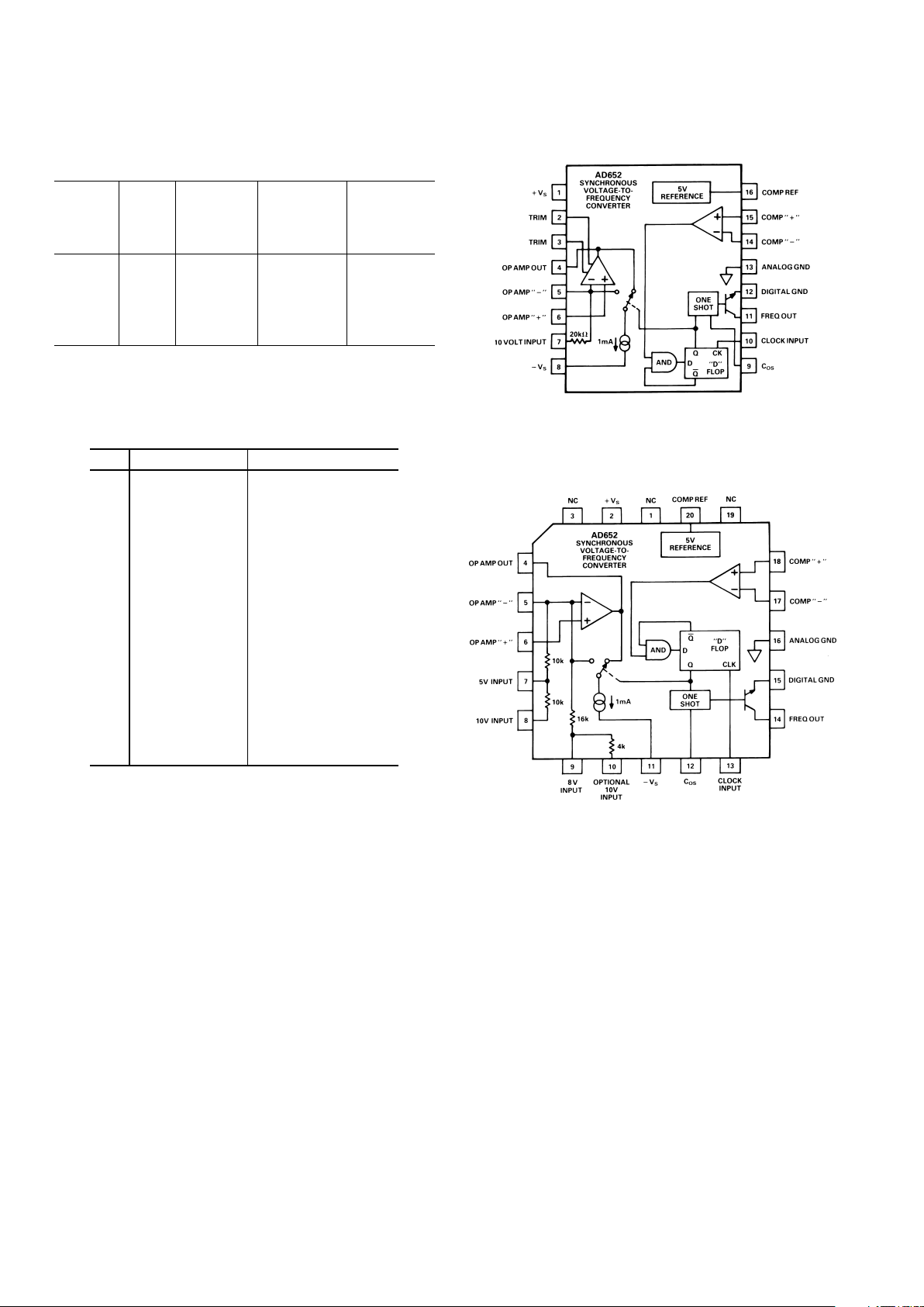
PIN CONFIGURATIONS
PIN Q-16 PACKAGE P-20A PACKAGE
1+V
S
NC
2 TRIM +V
S
3 TRIM NC
4 OP AMP OUT OP AMP OUT
5 OP AMP “—” OP AMP “—”
6 OP AMP “+” OP AMP “+”
7 10 VOLT INPUT 5 VOLT INPUT
8–V
S
10 VOLT INPUT
9C
OS
8 VOLT INPUT
10 CLOCK INPUT OPTIONAL 10 V INPUT
11 FREQ OUT –V
S
12 DIGITAL GND C
OS
13 ANALOG GND CLOCK INPUT
14 COMP “—” FREQ OUT
15 COMP “+“ DIGITAL GROUND
16 COMP REF ANALOG GND
17 COMP “—”
18 COMP “+”
19 NC
20 COMP REF
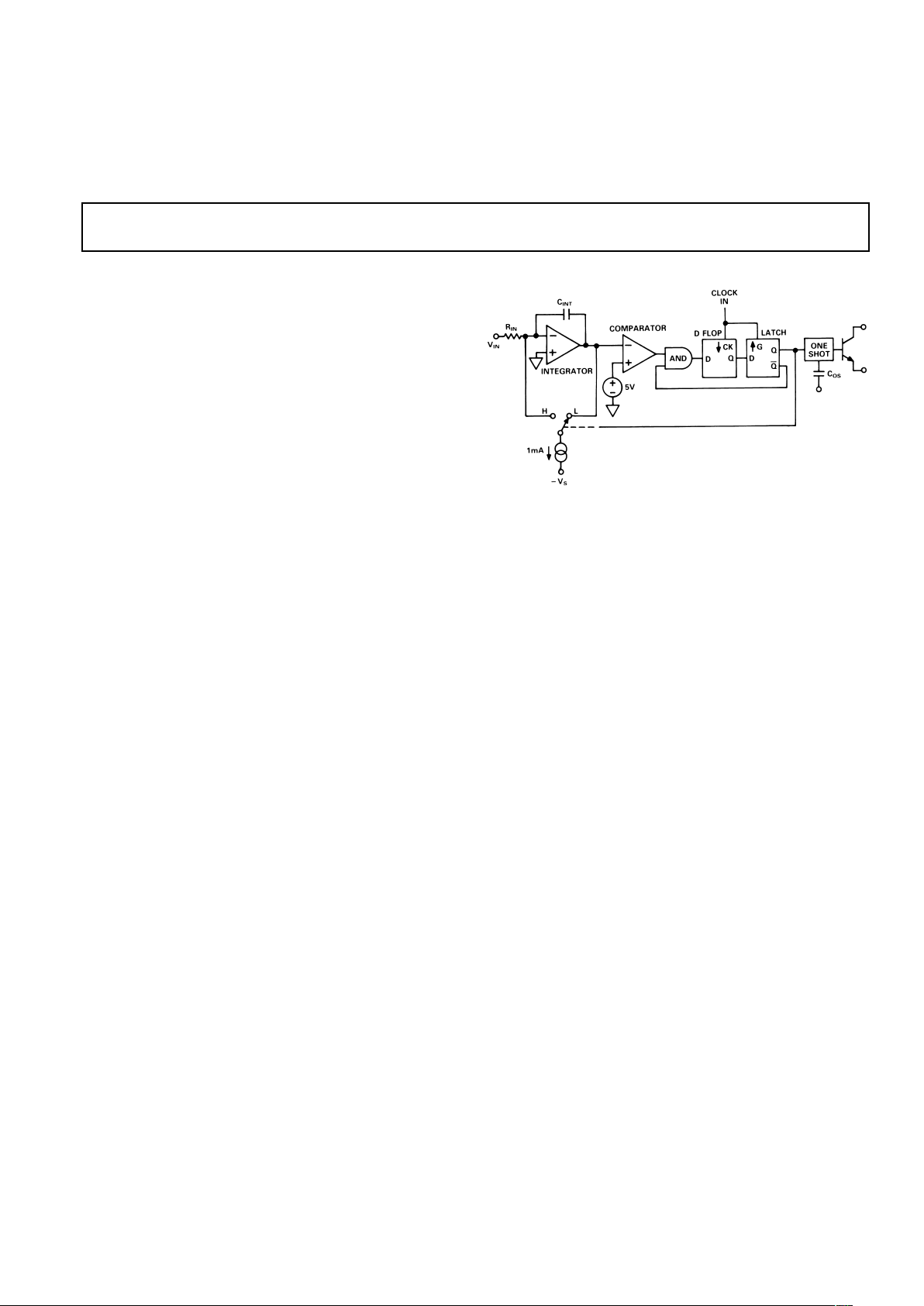
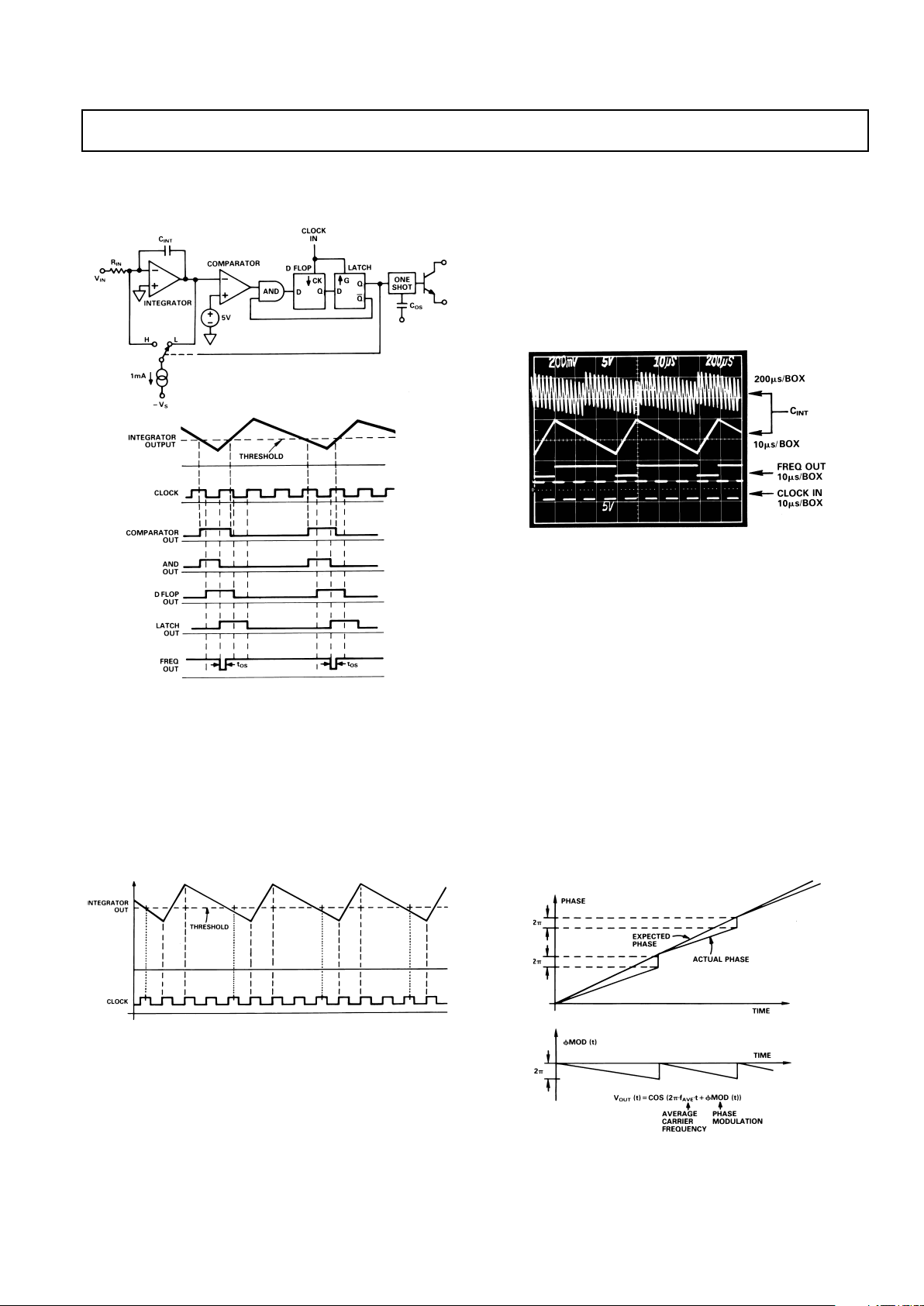
THEORY OF OPERATION
A synchronous VFC is similar to other voltage-to-frequency
converters in that an integrator is used to perform a chargebalance of the input signal with an internal reference current.
However, rather than using a one-shot as the primary timing
element which requires a high quality and low drift capacitor,
a synchronous voltage-to-frequency converter (SVFC) uses an
external clock; this allows the designer to determine the system
stability and drift based upon the external clock selected. A crystal oscillator may also be used if desired.
The SVFC architecture provides other system advantages besides
low drift. If the output frequency is measured by counting
pulses gated to a signal which is derived from the clock, the
clock stability is unimportant and the device simply performs as a
voltage controlled frequency divider, producing a high resolution
A/D. If a large number of inputs must be monitored simultaneously in a system, the controlled timing relationship between
the frequency output pulses and the user supplied clock greatly
simplifies this signal acquisition. Also, if the clock signal is provided by a VFC, then the output frequency of the SVFC will be
proportional to the product of the two input voltages.
Hence, multiplication and A-to-D conversion on two signals are
performed simultaneously.
Figure 1a. Cerdip Pin Configuration
The pinouts of the AD652 SVFC are shown in Figure 1. A
block diagram of the device configured as a SVFC, along with
various system waveforms, is shown in Figure 2.
Figure 1b. PLCC Pin Configuration
Figure 2 shows the typical up-and-down ramp integrator output
of a charge-balance VFC. After the integrator output has crossed
the comparator threshold and the output of the AND gate has
gone high, nothing happens until a negative edge of the clock
comes along to transfer the information to the output of the
D-FLOP. At this point, the clock level is low, so the latch does
not change state. When the clock returns high, the latch output
goes high and drives the switch to reset the integrator. At the
same time the latch drives the AND gate to a low output state.
On the very next negative edge of the clock the low output state
of the AND gate is transferred to the output of the D-FLOP
and then when the clock returns high, the latch output goes low
and drives the switch back into the Integrate Mode. At the same
time the latch drives the AND gate to a mode where it will truthfully relay the information presented to it by the comparator.
Since the reset pulses applied to the integrator are exactly one
clock period long, the only place where drift can occur is in a
variation of the symmetry of the switching speed with temperature. Since each reset pulse is identical to every other, the AD652
SVFC produces a very linear voltage to frequency transfer relation. Also, since all of the reset pulses are gated by the clock,
AD652
REV. B
–5–
there are no problems with dielectric absorption causing the
duration of a reset pulse to be influenced by the length of time
since the last reset.
Figure 2. AD652 Block Diagram and System Waveforms
Referring to Figure 2, it can be seen that the period between
output pulses is constrained to be an exact multiple of the clock
period. Consider an input current of exactly one quarter of the
value of the reference current. In order to achieve a charge balance, the output frequency will equal the clock frequency divided
by four; one clock period for reset and three clock periods of integrate. This is shown in Figure 3. If the input current is increased by
a very small amount, the output frequency should also increase
by a very small amount. Initially, however, no output change is
Figure 3. Integrator Output for lIN = 250 µA
observed for a very small increase in the input current. The output frequency continues to run at one quarter of the clock,
delivering an average of 250 µA to the summing junction. Since
the input current is slightly larger than this, charge accumulates
in the integrator and the sawtooth signal starts to drift downward.
As the integrator sawtooth drifts down, the comparator threshold is crossed earlier and earlier in each successive cycle, until
finally, a whole cycle is lost. When the cycle is lost, the Integrate
Phase lasts for two periods of the clock instead of the usual three
periods. Thus, among a long string of divide-by-fours an occasional
divide-by-three occurs; the average of the output frequency is
very close to one quarter of the clock, but the instantaneous frequency can be very different.
Because of this, it is very difficult to observe the waveform on an
oscilloscope. During all of this time, the signal at the output of
the integrator is a sawtooth wave with an envelope which is also
a sawtooth. This is shown in Figure 4.
Figure 4. Integrator Output for IIN Slightly Greater
than 250
µ
A
Another way to view this is that the output is a frequency of
approximately one quarter of the clock that has been phase
modulated. A constant frequency can be thought of as accumulating phase linearly with time at a rate equal to 2 πf radians per
second. Hence, the average output frequency which is slightly in
excess of a quarter of the clock will require phase accumulation
at a certain rate. However, since the SVFC is running at exactly
one quarter of the clock, it will not accumulate enough phase
(see Figure 5). When the difference between the required phase
(average frequency) and the actual phase equals 2 π, a step in
phase is taken where the deficit is made up instantaneously. The
output frequency is then a steady carrier which has been phase
modulated by a sawtooth signal (see Figure 5). The period of
the sawtooth phase modulation is the time required to accumulate
a 2 π difference in phase between the required average frequency
and one quarter of the clock frequency. The amplitude of the
sawtooth phase modulation is 2 π.
Figure 5. Phase Modulation
 Loading...