


UC2836N
Texas Instruments UC2836N, UC2836DW, UC2836DWTR, UC2836DTR, UC2836D Datasheet
...
FEATURES
• Complete Control for a High Current,
Low Dropout, Linear Regulator
• Fixed 5V or Adjustable Output Voltage
• Accurate 2.5A Current Limiting with
Foldback
• Internal Current Sense Resistor
• Remote Sense for Improved Load
Regulation
• External Shutdown
• Under-Voltage Lockout and Reverse
Voltage Protection
• Thermal Shutdown Protection
• 8 Pin Mini-Dip Package
(Surface Mount also Available)
DESCRIPTI ON
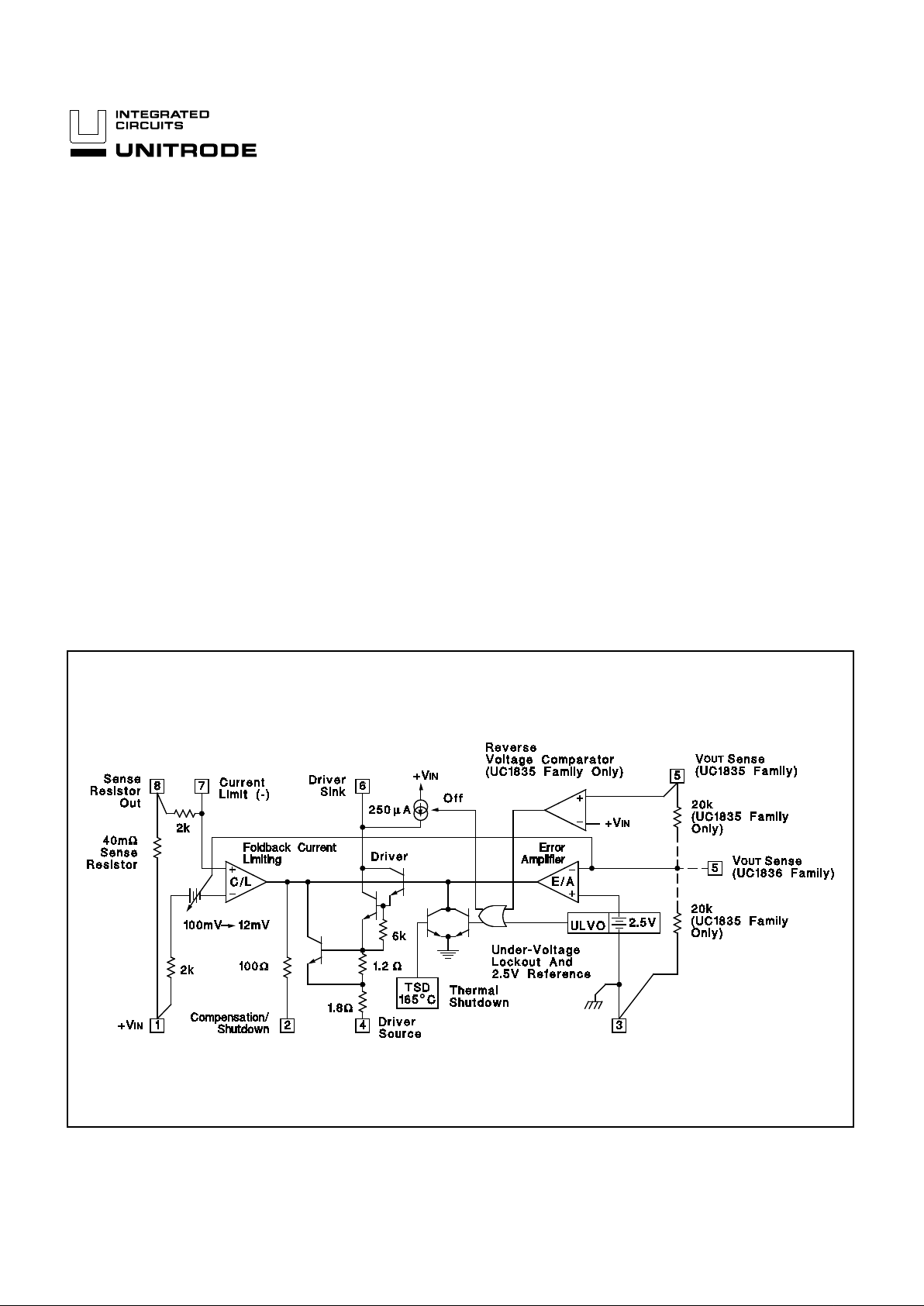
The UC1835/6 families of linear controllers are optimized for the design of low cost, low dropout, linear regulators. Using an external pass
element, dropout voltages of less than 0.5V are readily obtained.
These devices contain a high gain error amplifier, a 250mA output
driver, and a precision reference. I n addition, current sense with foldback provides for a 2.5A peak output current dropping to less than
0.5A at short circuit.
These devices are available in fixed, 5V, (UC1835), or adjustable,
(UC1836), versions. In the fi xed 5 volt version, the only external parts
required are an external pass element, an output capacitor, and a compensation capaci tor. On the adjustable version the output voltage can
be set anywhere from 2.5V to 35V with two external resistors.
Additional features of these devices include under-voltage lockout for
predictable start-up, thermal shutdown and short circuit current limiting
to protect the dri ver device. On the fixed voltage version, a reverse
voltage comparator mini mizes reverse load current in the event of a
negative input to output differential.
High Efficiency Regulator Controller
BLOCK DIAGRAM
Note: Pin numbers refer to 8-Pin DIL Pack age
UC1835 UC1836
UC2835 UC2836
UC3835 UC3836
8/94
UC1835 UC1836
UC2835 UC2836
UC3835 UC3836
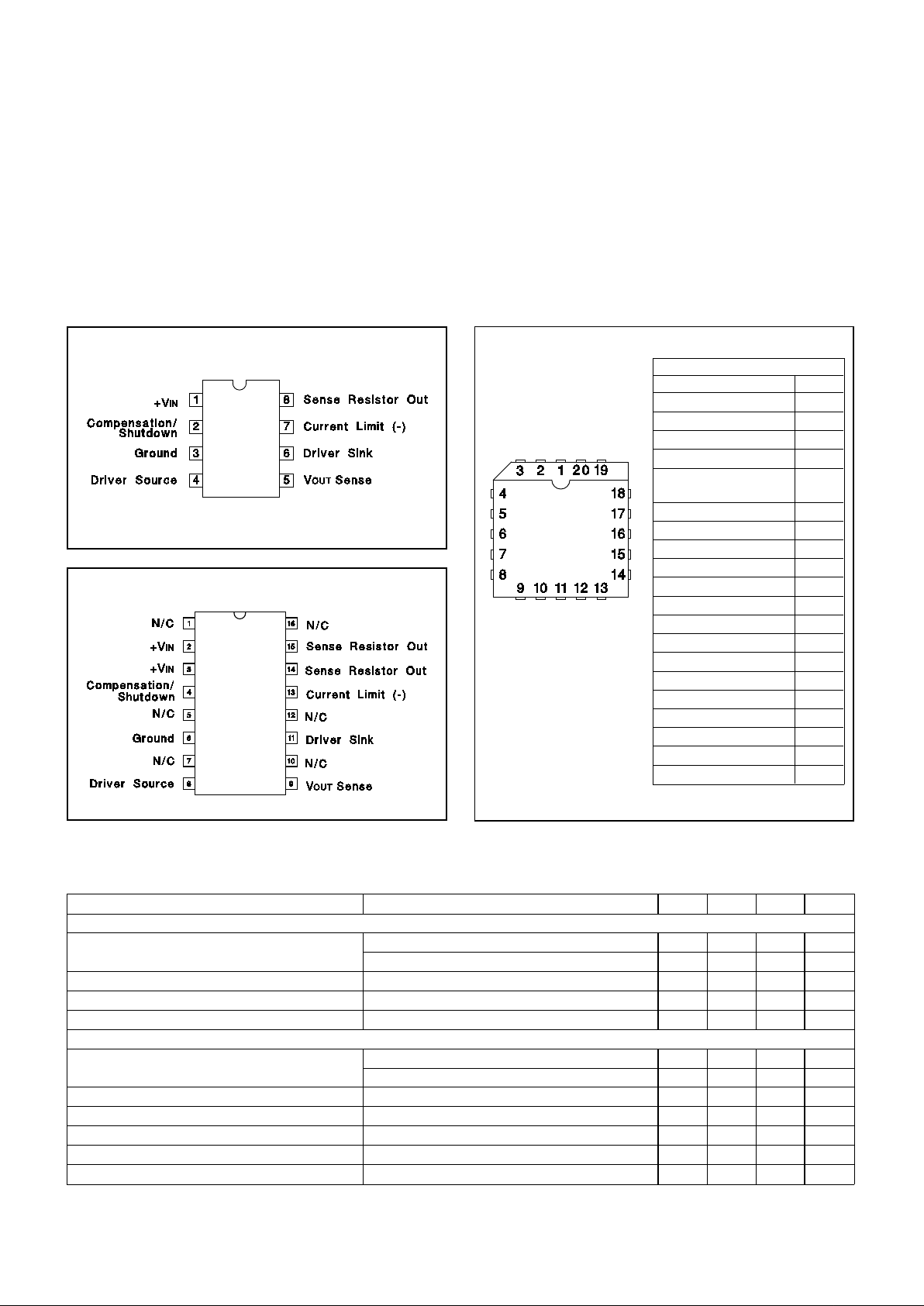
SOIC-16 (TOP VIEW)
DW Package
CONNECTION DIAGRAMS
PACKAGE PIN FUNCTION
FUNCTION PIN
N/C 1
+V
IN 2
+V
IN 3
N/C 4
Compensation/
Shutdown
5
N/C 6
Ground 7
N/C 8
N/C 9
Driver Source 10
N/C 11
V
OUT Sense 12
N/C 13
N/C 14
Driver Sink 15
N/C 16
Current Limit (-) 17
N/C 18
Sense Res isto r Out 19
Sense Res isto r Out 20
DIL-8, SOIC-8 (TOP VIEW)
N or J Package, D Package
PLCC-20, LCC-20
(TOP VIEW)
Q, L Packages
Input Supply Volt age ( +VIN) . . . . . . . . . . . . . . . . –1.0V to + 40V
Driver Outp ut Current (Sink or Source) . . . . . . . . . . . . . 600mA
Driver Sourc e to Sink Voltag e . . . . . . . . . . . . . . . . . . . . . + 40V
Maximum Curren t Throu gh Sens e Resist or. . . . . . . . . . . . . . 4A
V
OUT Sense Input Voltage . . . . . . . . . . . . . . . . . . –.3V to + 40V
Power Dissipation at T
A = 25°C (Note 2) . . . . . . . . . . . 1000mW
Power Dissipation at T
C = 25°C (Note 2). . . . . . . . . . . 2000mW
Operating Junct ion Te mp era tu re. . . . . . . . . . . -55°C to +150°C
Storage Temperature. . . . . . . . . . . . . . . . . . . . -65°C to +150°C
Lead Tempera tu re (Solderin g, 10 Seconds). . . . . . . . . . 300°C
Note 1: Voltages are refer ence d to grou nd, (Pin 3). Curre nt s are
positive into, negat ive ou t of, th e specified t er mina ls.
Consult Packaging Section of Datab ook for therma l
consideration s and limit ations of pac kage s.
ELECTRICAL CHARACTERISTICS:
Unless other wise stat ed, spe cifica tion s hold for TA = 0°C to + 70°C for the
UC3835/6, –25°C to + 85°C for the UC2835/6 , and –55°C to +12 5°C for the
UC1835/6, +V
IN = 6V, Driver Source= 0V, Drive r Sink = 5V, TA = TJ.
PARAMETER TEST CONDITIONS MIN. TYP. MAX. UNITS
Input Supply
Supply Current +V
IN = 6V 2.75 4.0 mA
+V
IN = 40V 3.75 6.0 mA
UVLO Threshold +V
IN Low to High, VOUT Sen se = 0 V 3.9 4.4 4.9 V
Threshold Hyster esis 0.1 0.35 V
Reverse Current +V
IN = -1.0V, Driver Sink Open 6.0 20 mA
Regulating Voltage an d Err or Ampl ifier (UC1835 Family Only)
Regulating Level at V
OUT Sense (VREG) Driver Current = 10mA, TJ = 25 ° C 4.94 5.0 5.06 V
Over Temperature 4.9 5.1 V
Line Regulation +V
IN = 5.2V + 35V 15 40 mV
Load Regulation Driver Current = 0 to 250mA 6. 0 25 mV
Bias Current at V
OUT Sense VOUT Sense = 5. 0 V 75 125 210 µA
Error Amp Transconductance ±100µA at Compensation/ Shut do wn P in 0.8 1.3 2.0 mS
Maximum Comp ensa tion Outp ut Current Sink or Source, Driver Source Open 90 200 260 µ A
ABSOLUTE MAXI MUM RATING S (Note 1)
2
 Loading...