


Texas Instruments UC2841N, UC2841J, UC2841DWTR, UC1841L883B, UC1841J883B Datasheet
...
UC1841
UC2841
UC3841
Programmable, Off-Line, PWM Controller
FEATURES
∙All Control, Driving, Monitoring, and Protection Functions Included
∙Low-current, Off-line Start Circuit
∙Voltage Feed Forward or Current Mode Control
∙Guaranteed Duty Cycle Clamp
∙PWM Latch for Single Pulse per Period
∙Pulse-by-Pulse Current Limiting Plus Shutdown for Over-Current Fault
∙No Start-up or Shutdown Transients
∙Slow Turn-on Both Initially and After Fault Shutdown
∙Shutdown Upon Overor Under-Voltage Sensing
∙Latch Off or Continuous Retry After Fault
∙PWM Output Switch Usable to 1A Peak Current
∙1% Reference Accuracy
∙500kHz Operation
∙18 Pin DIL Package
BLOCK DIAGRAM
DESCRIPTION
The UC1841 family of PWM controllers has been designed to increase the level of versatility while retaining all of the performance features of the earlier UC1840 devices. While still optimized for highly-efficient bootstrapped primary-side operation in forward or flyback power converters, the UC1841 is equally adept in implementing both low and high voltage input DC to DC converters. Important performance features include a low-current starting circuit, linear feed-forward for constant volt-second operation, and compatibility with either voltage or current mode topologies.
In addition to start-up and normal regulating PWM functions, these devices include built in protection from over-voltage, under-voltage, and over-current fault conditions with the option for either latch-off or automatic restart.
While pin compatible with the UC1840 in all respects except that the polarity of the External Stop has been reversed, the UC1841 offers the following improvements:
1.Fault latch reset is accomplished with slow start discharge rather than recycling the input voltage to the chip.
2.The External Stop input can be used for a fault delay to resist shutdown from short duration transients.
3.The duty-cycle clamping function has been characterized and specified.
The UC1841 is characterized for -55°C to +125°C operation while the UC2841 and UC3841 are designed for -25°C to +85°C and 0°to +70°C, respectively.
Note: Positive true logic, latch outputs high with set, reset has priority.
6/93
ABSOLUTE MAXIMUM RATINGS
Supply Voltage, +VIN (Pin 15) (Note 2)
Voltage Driven . . . . . . . . . . . . . . . . . . . . . . . . . . . . . . . . . +32V Current Driven, 100mA maximum . . . . . . . . . . . . Self-limiting PWM Output Voltage (Pin 12) . . . . . . . . . . . . . . . . . . . . . . . 40V PWM Output Current, Steady-State (Pin 12) . . . . . . . . . 400mA PWM Output Peak Energy Discharge . . . . . . . . . . . . 20μJoules Driver Bias Current (Pin 14) . . . . . . . . . . . . . . . . . . . . . -200mA Reference Output Current (Pin 16) . . . . . . . . . . . . . . . . -50mA Slow-Start Sink Current (Pin 8) . . . . . . . . . . . . . . . . . . . . 20mA VIN Sense Current (Pin 11). . . . . . . . . . . . . . . . . . . . . . . . 10mA Current Limit Inputs (Pins 6 & 7) . . . . . . . . . . . . . -0.5 to +5.5V Stop Input (Pin 4) . . . . . . . . . . . . . . . . . . . . . . . . . -0.3 to +5.5V
Comparator Inputs
(Pins 1, 7, 9-11, 16) . . . . . . . . . . . . Internally clamped at 12V Power Dissipation at TA = 25°C (Note 3) . . . . . . . . . . . 1000mW Power Dissipation at TC = 25°C (Note 3) . . . . . . . . . . . 2000mW
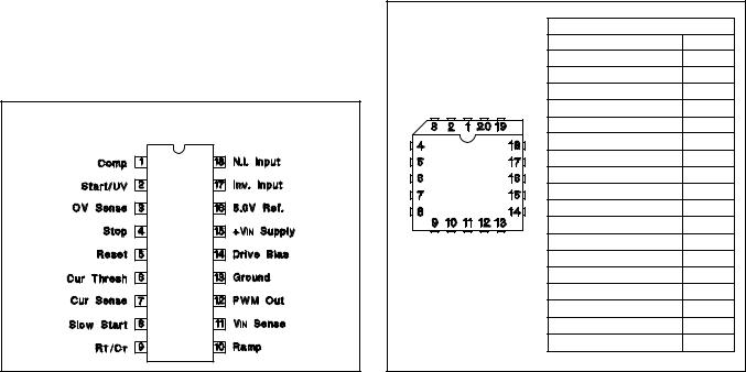
CONNECTION DIAGRAMS
DIL-18, SOIC-18 (TOP VIEW)
J or N, DW Package
UC1841
UC2841
UC3841
Operating Junction Temperature . . . . . . . . . . -55°C to +150°C Storage Temperature Range. . . . . . . . . . . . . . -65°C to +150°C Lead Temperature (Soldering, 10 sec) . . . . . . . . . . . . . +300°C
Note 1: All voltages are with respect to ground, Pin 13. Currents are positive-into, negative-out of the specified terminal.
Note 2: All pin numbers are referenced to DIL-18 package. Note 3: Consult Packaging Section of Databook for thermal limitations and considerations of package.
PLCC-20, LCC-20 |
PACKAGE PIN FUNCTIONS |
||
(TOP VIEW) |
|||
FUNCTION |
PIN |
||
Q or L Package |
|||
Comp |
1 |
||
|
|||
|
Start/UV |
2 |
|
|
OV Sense |
3 |
|
|
Stop |
4 |
|
|
Reset |
5 |
|
|
CUR Thresh |
7 |
|
|
CUR Sense |
8 |
|
|
Slow Start |
9 |
|
|
RT/CT |
10 |
|
|
Ramp |
11 |
|
|
VIN Sense |
12 |
|
|
PWM Out |
13 |
|
|
Ground |
14 |
|
|
Drive Bias |
15 |
|
|
+VIN Supply |
17 |
|
|
5.0V REF |
18 |
|
|
Inv. Input |
19 |
|
|
N.I. Input |
20 |
|
ELECTRICAL CHARACTERISTICS: Unless otherwise stated, these specifications apply for TA = -55°C to +125°C for the UC1841, -25°C to +85°C for the UC2841, and 0°C to +70°C for the UC3841; V IN = 20V, RT = 20kΩ, CT = .001mfd, RR = 10kΩ, CR = .001mfd, Current Limit Threshold = 200mV, TA = TJ.
PARAMETER |
TEST CONDITIONS |
UC1841 / UC2841 |
|
UC3841 |
|
UNITS |
|||
MIN |
TYP |
MAX |
MIN |
TYP |
|
MAX |
|
||
|
|
|
|
||||||
Power Inputs |
|
|
|
|
|
|
|
|
|
Start-Up Current |
VIN = 30V, Pin 2 = 2.5V |
|
4.5 |
6 |
|
4.5 |
|
6 |
mA |
Operating Current |
VIN = 30V, Pin 2 = 3.5V |
|
10 |
14 |
|
10 |
|
14 |
mA |
Supply OV Clamp |
IIN = 20mA |
33 |
40 |
45 |
33 |
40 |
|
45 |
V |
Reference Section |
|
|
|
|
|
|
|
|
|
Reference Voltage |
TJ = 25°C |
4.95 |
5.0 |
5.05 |
4.9 |
5.0 |
|
5.1 |
V |
Line Regulation |
VIN = 8 to 30V |
|
10 |
15 |
|
10 |
|
20 |
mV |
Load Regulation |
IL = 0 to 10mA |
|
10 |
20 |
|
10 |
|
30 |
mV |
Temperature Stability |
Over Operating Temperature Range |
4.9 |
|
5.1 |
4.85 |
|
|
5.15 |
V |
Short Circuit Current |
VREF = 0, TJ = 25°C |
|
-80 |
-100 |
|
-80 |
|
-100 |
mA |
Oscillator |
|
|
|
|
|
|
|
|
|
Nominal Frequency |
TJ = 25°C |
47 |
50 |
53 |
45 |
50 |
|
55 |
kHz |
Voltage Stability |
VIN = 8 to 30V |
|
0.5 |
1 |
|
0.5 |
|
1 |
% |
Temperature Stability |
Over Operating Temperature Range |
45 |
|
55 |
43 |
|
|
57 |
kHz |
Maximum Frequency |
RT = 2kΩ, CT = 330pF |
500 |
|
|
500 |
|
|
|
kHz |
|
|
|
|
|
|
|
|
|
|
2
UC1841
UC2841
UC3841
ELECTRICAL CHARACTERISTICS: Unless otherwise stated, these specifications apply for TA = -55°C to +125°C for the UC1841, -25°C to +85°C for the UC2841, and 0°C to +70°C for the UC3841; V IN = 20V, RT = 20kΩ, CT = .001mfd, RR = 10kΩ, CR = .001mfd, Current Limit Threshold = 200mV, TA = TJ.
PARAMETER |
TEST CONDITIONS |
UC1841 / UC2841 |
|
UC3841 |
|
UNITS |
|||
|
|
MIN |
TYP |
MAX |
MIN |
TYP |
|
MAX |
|
Ramp Generator |
|
|
|
|
|
|
|
|
|
Ramp Current, Minimum |
ISENSE = -10μA |
|
-11 |
-14 |
|
-11 |
|
-14 |
μA |
Ramp Current, Maximum |
ISENSE = 1.0mA |
-0.9 |
-.95 |
|
-0.9 |
-.95 |
|
|
mA |
Ramp Valley |
|
0.3 |
0.4 |
0.6 |
0.3 |
0.4 |
|
0.6 |
V |
Ramp Peak |
Clamping Level |
3.9 |
4.2 |
4.5 |
3.9 |
4.2 |
|
4.5 |
V |
Error Amplifier |
|
|
|
|
|
|
|
|
|
Input Offset Voltage |
VCM = 5.0V |
|
0.5 |
5 |
|
2 |
|
10 |
mV |
Input Bias Current |
|
|
0.5 |
2 |
|
1 |
|
5 |
μA |
Input Offset Current |
|
|
|
0.5 |
|
|
|
0.5 |
μA |
Open Loop Gain |
VO= 1 to 3V |
60 |
66 |
|
60 |
66 |
|
|
dB |
Output Swing (Max. Output ≤ |
Minimum Total Range |
0.3 |
|
3.5 |
0.3 |
|
|
3.5 |
V |
Ramp Peak - 100mV) |
|
|
|
|
|
|
|
|
|
CMRR |
VCM = 1.5 to 5.5V |
70 |
80 |
|
70 |
80 |
|
|
dB |
PSRR |
VIN = 8 to 30V |
70 |
80 |
|
70 |
80 |
|
|
dB |
Short Circuit Current |
VCOMP = 0V |
|
-4 |
-10 |
|
-4 |
|
-10 |
mA |
Gain Bandwidth* |
TJ = 25°C, A VOL = 0dB |
1 |
2 |
|
1 |
2 |
|
|
MHz |
Slew Rate* |
TJ = 25°C, A VCL = 0dB |
|
0.8 |
|
|
0.8 |
|
|
V/μs |
PWM Section |
|
|
|
|
|
|
|
|
|
Continuous Duty Cycle |
Minimum Total Continuous Range, |
4 |
|
95 |
4 |
|
|
95 |
% |
Range* (other than zero) |
Ramp Peak < 4.2V |
|
|
|
|
|
|
|
|
50% Duty Cycle Clamp |
RSENSE to VREF = 10k |
42 |
47 |
52 |
42 |
47 |
|
52 |
% |
Output Saturation |
IOUT = 20mA |
|
0.2 |
0.4 |
|
0.2 |
|
0.4 |
V |
|
IOUT = 200mA |
|
1.7 |
2.2 |
|
1.7 |
|
2.2 |
V |
Output Leakage |
VOUT = 40V |
|
0.1 |
10 |
|
0.1 |
|
10 |
μA |
Comparator Delay* |
Pin 8 to Pin 12, TJ = 25°C, RL = 1kΩ |
|
300 |
500 |
|
300 |
|
500 |
ns |
Sequencing Functions |
|
|
|
|
|
|
|
|
|
Comparator Thresholds |
Pins 2, 3, 5 |
2.8 |
3.0 |
3.2 |
2.8 |
3.0 |
|
3.2 |
V |
Input Bias Current |
Pins 3, 5 = 0V |
|
-1.0 |
-4.0 |
|
-1.0 |
|
-4.0 |
μA |
Input Leakage |
Pins 3, 5 = 10V |
|
0.1 |
2.0 |
|
0.1 |
|
2.0 |
μA |
Start/UV Hysteresis Current |
Pin 2 = 2.5V |
170 |
200 |
220 |
170 |
200 |
|
230 |
μA |
Ext. Stop Threshold |
Pin 4 |
0.8 |
1.6 |
2.4 |
0.8 |
1.6 |
|
2.4 |
V |
Error Latch Activate Current |
Pin 4 = 0V, Pin 3 > 3V |
|
-120 |
-200 |
|
-120 |
|
-200 |
μA |
Driver Bias Saturation Voltage, |
IB = -50mA |
|
2 |
3 |
|
2 |
|
3 |
V |
VIN - VOH |
|
|
|
|
|
|
|
|
|
Driver Bias Leakage |
VB = 0V |
|
-0.1 |
-10 |
|
-0.1 |
|
-10 |
μA |
Slow-Start Saturation |
IS = 10mA |
|
0.2 |
0.5 |
|
0.2 |
|
0.5 |
V |
Slow-Start Leakage |
VS = 4.5V |
|
0.1 |
2.0 |
|
0.1 |
|
2.0 |
μA |
Current Control |
|
|
|
|
|
|
|
|
|
Current Limit Offset |
|
|
0 |
5 |
|
0 |
|
10 |
mV |
Current Shutdown Offset |
|
370 |
400 |
430 |
360 |
400 |
|
440 |
mV |
Input Bias Current |
Pin 7 = 0V |
|
-2 |
-5 |
|
-2 |
|
-5 |
μA |
Common Mode Range* |
|
-0.4 |
|
3.0 |
-0.4 |
|
|
3.0 |
V |
Current Limit Delay* |
TJ = 25°C, Pin 7 to 12, RL = 1k |
|
200 |
400 |
|
200 |
|
400 |
ns |
* These parameters are guaranteed by design but not 100% tested in production.
3
 Loading...