


TEXAS INSTRUMENTS UC1842A, UC1843A, UC1844A, UC1845A, UC2842A Technical data
...application
INFO
available
UC1842A/3A/4A/5A
UC2842A/3A/4A/5A
UC3842A/3A/4A/5A
Current Mode PWM Controller
FEATURES
•Optimized for Off-line and DC to DC Converters
•Low Start Up Current (<0.5mA)
•Trimmed Oscillator Discharge Current
•Automatic Feed Forward Compensation
•Pulse-by-Pulse Current Limiting
•Enhanced Load Response Characteristics
•Under-Voltage Lockout With Hysteresis
•Double Pulse Suppression
•High Current Totem Pole Output
•Internally Trimmed Bandgap Reference
•500kHz Operation
•Low RO Error Amp
DESCRIPTION
The UC1842A/3A/4A/5A family of control ICs is a pin for pin compatible improved version of the UC3842/3/4/5 family. Providing the necessary features to control current mode switched mode power supplies, this family has the following improved features. Start up current is guaranteed to be less than 0.5mA. Oscillator discharge is trimmed to 8.3mA. During under voltage lockout, the output stage can sink at least 10mA at less than 1.2V for VCC over 5V.
The difference between members of this family are shown in the table below.
Part # |
UVLO On |
UVLO Off |
Maximum Duty |
|
Cycle |
||||
|
|
|
||
UC1842A |
16.0V |
10.0V |
<100% |
|
UC1843A |
8.5V |
7.9V |
<100% |
|
UC1844A |
16.0V |
10.0V |
<50% |
|
UC1845A |
8.5V |
7.9V |
<50% |
BLOCK DIAGRAM
Note 1: A/B A = DIL-8 Pin Number. B = SO-14 Pin Number. Note 2: Toggle flip flop used only in 1844A and 1845A.
SLUS224A - SEPTEMBER 1994 - REVISED APRIL 2002

|
|
|
UC1842A/3A/4A/5A |
|
|
CONNECTION DIAGRAMS |
UC2842A/3A/4A/5A |
||
|
|
|
UC3842A/3A/4A/5A |
|
ABSOLUTE MAXIMUM RATINGS (Note 1) |
|
|
|
|
Supply Voltage (Low Impedance Source) . . . . |
. . . . . . . . . . 30V |
PLCC-20, LCC-20 |
|
|
Supply Voltage (ICC mA) . . . . . . . . . . . . . . . . . |
. . . Self Limiting |
(TOP VIEW) |
|
|
Output Current. . . . . . . . . . . . . . . . . . . . . . . . . . |
. . . . . . . . . ±1A |
Q, L Packages |
|
|
Output Energy (Capacitive Load). . . . . . . . . . . . |
. . . . . . . . . 5 J |
|
|
|
|
|
|
PACKAGE PIN FUNCTION |
|
Analog Inputs (Pins 2, 3). . . . . . . . . . . . . . . . . . . |
-0.3V to +6.3V |
|
FUNCTION |
PIN |
Error Amp Output Sink Current . . . . . . . . . . . . . |
. . . . . . . 10mA |
|
N/C |
1 |
Power Dissipation at TA ≤ 25°C (DIL-8) . . . . . . . |
. . . . . . . . . 1W |
|
Comp |
2 |
Storage Temperature Range. . . . . . . . . . . . . . |
- 65°C to +150°C |
|
N/C |
3-4 |
|
|
|
VFB |
5 |
Lead Temperature (Soldering, 10 Seconds) . . . |
. . . . . . . 300°C |
|
|
|
|
|
|
N/C |
6 |
Note 1. All voltages are with respect to Ground, Pin 5. Currents |
|
|
|
|
|
|
|
ISENSE |
7 |
are positive into, negative out of the specified terminal. Consult |
|
|
|
|
|
|
|
N/C |
8-9 |
Packaging Section of Databook for thermal limitations and con- |
|
|
|
|
|
|
|
RT/CT |
10 |
siderations of packages. Pin numbers refer to DIL package only. |
|
|
|
|
|
|
|
N/C |
11 |
|
|
|
Pwr Gnd |
12 |
SOIC-14 (TOP VIEW) |
|
|
|
|
|
|
|
Gnd |
13 |
D Package |
|
|
|
|
|
|
|
N/C |
14 |
|
|
|
Output |
15 |
|
|
|
N/C |
16 |
|
|
|
VC |
17 |
|
|
|
VCC |
18 |
|
|
|
N/C |
19 |
|
|
|
VREF |
20 |
DIL-8, SOIC-8 (TOP VIEW)
J or N, D8 Package
SOIC-WIDE16 (TOP VIEW) |
|
|
||||
DW Package |
|
|
|
|
|
|
N/C |
|
|
|
|
|
N/C |
1 |
|
|
|
16 |
||
N/C |
|
|
|
|
|
|
|
|
|
|
|
|
|
2 |
|
|
|
15 |
VREF |
|
COMP |
|
|
|
|
|
VCC |
|
|
|
|
|
||
3 |
|
|
|
14 |
||
VFB |
|
|
|
|
|
|
|
|
|
|
|
|
|
4 |
|
|
|
13 |
VCC |
|
ISENSE |
|
|
|
|
|
|
|
|
|
|
|
|
|
5 |
|
|
|
12 |
OUTPUT |
|
RT/CT |
|
|
|
|
|
GND |
|
|
|
|
|
||
6 |
|
|
|
11 |
||
N/C |
|
|
|
|
|
|
|
|
|
|
|
|
|
7 |
|
|
|
10 |
PWRGND |
|
|
|
|
|
|
|
|
|
|
|
|
|
|
|
N/C |
8 |
|
|
|
9 |
N/C |
|
|
|
|
|
|
|
|
|
|
|
|
|
|
|
|
|
|
|
|
|
2
UC1842A/3A/4A/5A
UC2842A/3A/4A/5A
UC3842A/3A/4A/5A
ELECTRICAL CHARACTERISTICS Unless otherwise stated, these specifications apply for –55°C ≤ TA ≤ 125°C for the UC184xA; –40°C ≤ TA ≤ 125°C for the UC284xAQ; –40°C ≤ TA ≤ 85°C for the UC284xA; 0 ≤ TA ≤ 70°C for the UC384xA; VCC = 15V (Note 5); RT = 10k; CT = 3.3nF; TA = TJ; Pin numbers refer to DIL-8.
PARAMETER |
TEST CONDITIONS |
UC184xA\UC284xA |
|
UC384xA |
|
UNITS |
|||||
MIN. |
TYP. |
MAX. |
MIN. |
TYP. |
MAX. |
||||||
|
|
|
|||||||||
Reference Section |
|
|
|
|
|
|
|
|
|
|
|
Output Voltage |
TJ = 25°C, IO = 1mA |
4.95 |
5.00 |
5.05 |
4.90 |
|
5.00 |
|
5.10 |
V |
|
Line Regulation |
12 ≤ VIN 25V |
|
6 |
20 |
|
|
6 |
|
20 |
mV |
|
Load Regulation |
1 ≤ IO ≤ 20mA |
|
6 |
25 |
|
|
6 |
|
25 |
mV |
|
Temp. Stability |
(Note 2, Note 7) |
|
0.2 |
0.4 |
|
|
0.2 |
|
0.4 |
mV/°C |
|
Total Output Variation |
Line, Load, Temp. |
4.9 |
|
5.1 |
4.82 |
|
|
|
5.18 |
V |
|
Output Noise Voltage |
10Hz ≤ f ≤ 10kHz |
|
|
|
|
|
|
|
|
|
|
|
TJ = 25°C (Note 2) |
|
50 |
|
|
|
50 |
|
|
V |
|
Long Term Stability |
TA = 125°C, 1000Hrs. (Note 2) |
|
5 |
25 |
|
|
5 |
|
25 |
mV |
|
Output Short Circuit |
|
-30 |
-100 |
-180 |
-30 |
|
-100 |
|
-180 |
mA |
|
Oscillator Section |
|
|
|
|
|
|
|
|
|
|
|
Initial Accuracy |
TJ = 25°C (Note 6) |
47 |
52 |
57 |
47 |
|
52 |
|
57 |
kHz |
|
Voltage Stability |
12 ≤ VCC ≤ 25V |
|
0.2 |
1 |
|
|
0.2 |
|
1 |
% |
|
Temp. Stability |
TMIN ≤ TA ≤ TMAX (Note 2) |
|
5 |
|
|
|
5 |
|
|
% |
|
Amplitude |
VPIN 4 peak to peak (Note 2) |
|
1.7 |
|
|
|
1.7 |
|
|
V |
|
Discharge Current |
TJ = 25°C, VPIN 4 = 2V (Note 8) |
7.8 |
8.3 |
8.8 |
7.8 |
|
8.3 |
|
8.8 |
mA |
|
|
VPIN 4 = 2V (Note 8) |
7.5 |
|
8.8 |
7.6 |
|
|
|
8.8 |
mA |
|
Error Amp Section |
|
|
|
|
|
|
|
|
|
|
|
Input Voltage |
VPIN 1 = 2.5V |
2.45 |
2.50 |
2.55 |
2.42 |
|
2.50 |
|
2.58 |
V |
|
Input Bias Current |
|
|
-0.3 |
-1 |
|
|
-0.3 |
|
-2 |
A |
|
AVOL |
2 ≤ VO ≤ 4V |
65 |
90 |
|
65 |
|
90 |
|
|
dB |
|
Unity Gain Bandwidth |
TJ = 25°C (Note 2) |
0.7 |
1 |
|
0.7 |
|
1 |
|
|
MHz |
|
PSRR |
12 ≤ VCC ≤ 25V |
60 |
70 |
|
60 |
|
70 |
|
|
dB |
|
Output Sink Current |
VPIN 2 = 2.7V, VPIN 1 = 1.1V |
2 |
6 |
|
2 |
|
6 |
|
|
mA |
|
Output Source Current |
VPIN 2 = 2.3V, VPIN 1 = 5V |
-0.5 |
-0.8 |
|
-0.5 |
|
-0.8 |
|
|
mA |
|
VOUT High |
VPIN 2 = 2.3V, RL = 15k to ground |
5 |
6 |
|
5 |
|
6 |
|
|
V |
|
VOUT Low |
VPIN 2 = 2.7V, RL = 15k to Pin 8 |
|
0.7 |
1.1 |
|
|
0.7 |
|
1.1 |
V |
|
Current Sense Section |
|
|
|
|
|
|
|
|
|
|
|
Gain |
(Note 3, Note 4) |
2.85 |
3 |
3.15 |
2.85 |
|
3 |
|
3.15 |
V/V |
|
Maximum Input Signal |
VPIN 1 = 5V (Note 3) |
0.9 |
1 |
1.1 |
0.9 |
|
1 |
|
1.1 |
V |
|
PSRR |
12 ≤ VCC ≤ 25V (Note 3) |
|
70 |
|
|
|
70 |
|
|
dB |
|
Input Bias Current |
|
|
-2 |
-10 |
|
|
-2 |
|
-10 |
A |
|
Delay to Output |
VPIN 3 = 0 to 2V (Note 2) |
|
150 |
300 |
|
|
150 |
|
300 |
ns |
|
Output Section |
|
|
|
|
|
|
|
|
|
|
|
Output Low Level |
ISINK = 20mA |
|
0.1 |
0.4 |
|
|
0.1 |
|
0.4 |
V |
|
|
ISINK = 200mA |
|
15 |
2.2 |
|
|
15 |
|
2.2 |
V |
|
Output High Level |
ISOURCE = 20mA |
13 |
13.5 |
|
13 |
|
13.5 |
|
|
V |
|
|
ISOURCE = 200mA |
12 |
13.5 |
|
12 |
|
13.5 |
|
|
V |
|
Rise Time |
TJ = 25°C, CL = 1nF (Note 2) |
|
50 |
150 |
|
|
50 |
|
150 |
ns |
|
Fall Time |
TJ = 25°C, CL = 1nF (Note 2) |
|
50 |
150 |
|
|
50 |
|
150 |
ns |
|
UVLO Saturation |
VCC = 5V, ISINK = 10mA |
|
0.7 |
1.2 |
|
|
0.7 |
|
1.2 |
V |
|
3

UC1842A/3A/4A/5A
UC2842A/3A/4A/5A
UC3842A/3A/4A/5A
ELECTRICAL CHARACTERISTICS Unless otherwise stated, these specifications apply for –55°C ≤ TA ≤ 125°C for the UC184xA; –40°C ≤ TA ≤ 125°C for the UC284xAQ; –40°C ≤ TA ≤ 85°C for the UC284xA; 0 ≤ TA ≤ 70°C for the UC384xA; VCC = 15V (Note 5); RT = 10k; CT = 3.3nF; TA = TJ; Pin numbers refer to DIL-8.
PARAMETER |
TEST CONDITIONS |
UC184xA\UC284xA |
|
UC384xA |
|
UNITS |
|||||
MIN. |
TYP. |
MAX. |
MIN. |
TYP. |
MAX. |
||||||
|
|
|
|||||||||
Under-Voltage Lockout Section |
|
|
|
|
|
|
|
|
|
|
|
Start Threshold |
x842A/4A |
15 |
16 |
17 |
14.5 |
|
16 |
|
17.5 |
V |
|
|
x843A/5A |
7.8 |
8.4 |
9.0 |
7.8 |
|
8.4 |
|
9.0 |
V |
|
Min. Operation Voltage After |
x842A/4A |
9 |
10 |
11 |
8.5 |
|
10 |
|
11.5 |
V |
|
Turn On |
x843A/5A |
7.0 |
7.6 |
8.2 |
7.0 |
|
7.6 |
|
8.2 |
V |
|
PWM Section |
|
|
|
|
|
|
|
|
|
|
|
Maximum Duty Cycle |
x842A/3A |
94 |
96 |
100 |
94 |
|
96 |
|
100 |
% |
|
|
x844A/5A |
47 |
48 |
50 |
47 |
|
48 |
|
50 |
% |
|
Minimum Duty Cycle |
|
|
|
0 |
|
|
|
|
0 |
% |
|
Total Standby Current |
|
|
|
|
|
|
|
|
|
|
|
Start-Up Current |
|
|
0.3 |
0.5 |
|
|
0.3 |
|
0.5 |
mA |
|
Operating Supply Current |
VPIN 2 = VPIN 3 = 0V |
|
11 |
17 |
|
|
11 |
|
17 |
mA |
|
VCC Zener Voltage |
ICC = 25mA |
30 |
34 |
|
30 |
|
34 |
|
|
V |
|
Note 2: Ensured by design, but not 100% production tested.
Note 3: Parameter measured at trip point of latch with VPIN2 = 0.
Note 4: Gain defined as: A = ∆VPIN 1 ; 0  VPIN 3
  0.8V. ∆VPIN 3
Note 5: Adjust VCC above the start threshold before setting at 15V.
Note 6: Output frequency equals oscillator frequency for the UC1842A and UC1843A. Output frequency is one half oscillator frequency for the UC1844A and UC1845A.
Note 7: “Temperature stability, sometimes referred to as average temperature coefficient, is described by the equation:
Temp Stability = VREF (max ) − VREF (min).VREF (max) and VREF (min) are the maximum & minimum reference voltTJ (max ) − TJ (min)
age measured over the appropriate temperature range. Note that the extremes in voltage do not necessarily occur at the extremes in temperature.”
Note 8: This parameter is measured with RT = 10k to VREF.This contributes approximately 300
 A of current to the measurement. The total current flowing into the RT/C pin will be approximately 300
 A higher than the measured value.
Error Amp Configuration
Error Amp can Source and Sink up to 0.5mA, and Sink up to 2mA.
4
UC1842A/3A/4A/5A
UC2842A/3A/4A/5A
UC3842A/3A/4A/5A
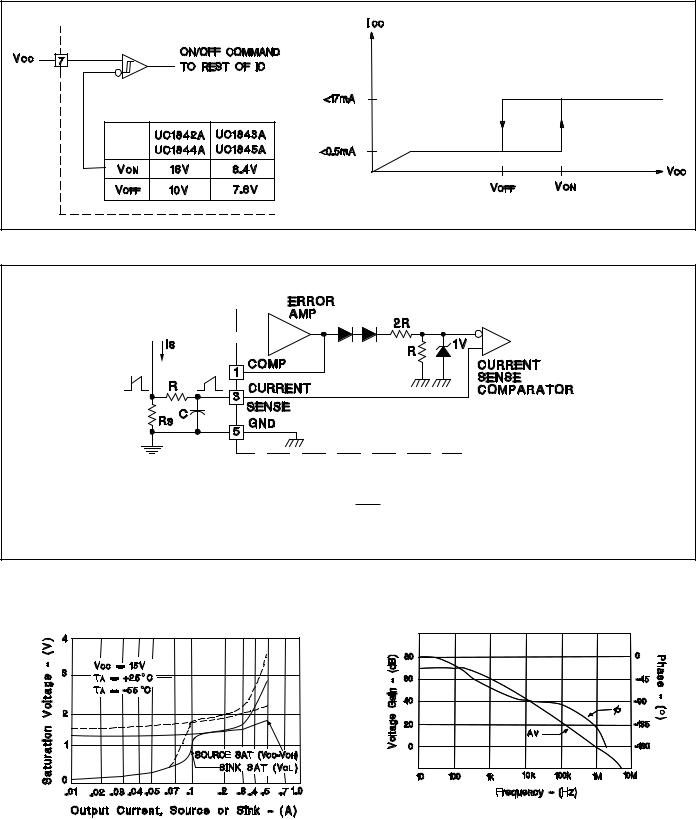
Under-Voltage Lockout
During UVLO, the Output is low.
Current Sense Circuit
Peak Current (IS) is Determined By The Formula
′ 1.0V
ISMAX
RS
A small RC filter may be required to suppress switch transients.
Output Saturation Characteristics |
Error Amplifier Open-Loop Frequency Response |
||||||||||||||||||||||||
|
|
|
|
|
|
|
|
|
|
|
|
|
|
|
|
|
|
|
|
|
|
|
|
|
|
|
|
|
|
|
|
|
|
|
|
|
|
|
|
|
|
|
|
|
|
|
|
|
|
|
|
|
|
|
|
|
|
|
|
|
|
|
|
|
|
|
|
|
|
|
|
|
|
|
|
|
|
|
|
|
|
|
|
|
|
|
|
|
|
|
|
|
|
|
|
|
|
|
|
|
|
|
|
|
|
|
|
|
|
|
|
|
|
|
|
|
|
|
|
|
|
|
|
|
|
|
|
|
|
|
|
|
|
|
|
|
|
|
|
|
|
|
|
|
|
|
|
|
|
|
|
|
|
|
|
|
|
|
|
|
|
|
|
|
|
|
|
|
|
|
|
|
|
|
|
|
|
|
|
|
|
|
|
|
|
|
|
|
|
|
|
|
|
|
|
|
|
|
|
|
|
|
|
|
|
|
|
5

UC1842A/3A/4A/5A
UC2842A/3A/4A/5A
APPLICATIONS DATA (cont.)
Oscillator Section
Oscillator Frequency vs Timing Resistance |
Maximum Duty Cycle vs Timing Resistor |
Open-Loop Laboratory Test Fixture
High peak currents associated with capacitive loads necessitate careful grounding techniques. Timing and bypass capacitors should be connected close to pin 5 in a single point
ground. The transistor and 5k potentiometer are used to sample the oscillator waveform and apply an adjustable ramp to pin 3.
Slope Compensation
A fraction of the oscillator ramp can be resistively summed with the current sense signal to provide slope compensation for converters requiring duty cycles over 50%.
Note that capacitor, C, forms a filter with R2 to suppress the leading edge switch spikes.
6
|
UC1842A/3A/4A/5A |
|
UC2842A/3A/4A/5A |
APPLICATIONS DATA (cont.) |
UC3842A/3A/4A/5A |
|
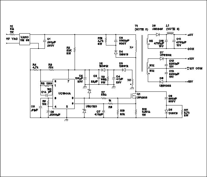
Off-line Flyback Regulator
Power Supply Specifications |
|
5. Output Voltage: |
||
1. Input Voltage |
|
95VAC to 130VA |
A. +5V, ±5%; 1A to 4A load |
|
|
Ripple voltage: 50mV P-P Max |
|||
|
|
(50 Hz/60Hz) |
||
|
|
B. +12V, ±3%; 0.1A to 0.3A load |
||
2. Line Isolation |
|
3750V |
||
|
Ripple voltage: 100mV P-P Max |
|||
3. Switching Frequency |
40kHz |
|||
C. -12V ,±3%; 0.1A to 0.3A load |
||||
4. Efficiency |
Full Load |
70% |
||
Ripple voltage: 100mV P-P Max |
||||
|
|
|
||
7
 Loading...