


UC1856 UC2856 UC3856
Improved Current Mode PWM Controller
FEATURES |
DESCRIPTION |
•Pin-for-Pin Compatible With the UC3846 The UC3856 is a high performance version of the popular UC3846
•65ns Typical Delay From Shutdown to Outputs, and 50ns Typical Delay From Sync to Outputs
•Improved Current Sense Amplifier With Reduced Noise Sensitivity
•Differential Current Sense with 3V Common Mode Range
•Trimmed Oscillator Discharge Current for Accurate Deadband Control
•Accurate 1V Shutdown Threshold
•High Current Dual Totem Pole Outputs (1.5A peak)
•TTL Compatible Oscillator SYNC Pin Thresholds
•4kV ESD Protection
series of current mode controllers, and is intended for both design upgrades and new applications where speed and accuracy are important. All input to output delays have been minimized, and the current sense output is slew rate limited to reduce noise sensitivity. Fast 1.5A peak output stages have been added to allow rapid switching of power FETs.
A low impedance TTL compatible sync output has been implemented with a tri-state function when used as a sync input.
Internal chip grounding has been improved to minimize internal “noise” caused when driving large capacitive loads. This, in conjunction with the improved differential current sense amplifier results in enhanced noise immunity.
Other features include a trimmed oscillator current (8%) for accurate frequency and dead time control; a 1V, 5% shutdown threshold; and 4kV minimum ESD protection on all pins.
BLOCK DIAGRAM
UDG-96176
9/96
ABSOLUTE MAXIMUM RATINGS
Supply Voltage .................................................................... |
+40V |
Collector Supply Voltage ..................................................... |
+40V |
Output Current, Source or Sink |
|
DC................................................................................... |
0.5A |
Pulse (0.5μs)................................................................... |
2.0A |
Error Amp Inputs.................................................... |
−0.3V to +VIN |
Shutdown Input..................................................... |
−0.3V to +10V |
Current Sense Inputs.............................................. |
−0.3V to +3V |
SYNC Output Current ...................................................... |
±10mA |
Error Amplifier Output Current ........................................... |
−5mA |
Soft Start Sink Current....................................................... |
50mA |
Oscillator Charging Current ................................................. |
5mA |
Power Dissipation at TA = 25°C (Note 2)....................... |
1000mW |
Power Dissipation at TC = 25°C (Note 2) ...................... |
2000mW |
Junction Temperature ....................................... |
−55°C to +150°C |
Storage Temperature Range ............................ |
−65°C to +150°C |
Lead Temperature (Soldering, 10 sec.) ........................... |
+300°C |
All voltages are with respect to Ground. Currents are positive into, negative out of the specified terminal. Consult packaging section of databook for thermal limitations and considerations of package.
UC1856
UC2856
UC3856
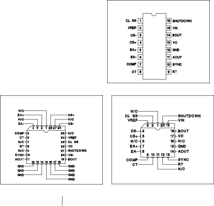
CONNECTION DIAGRAMS
DIL–16, SOIC-16 (Top View)
J or N, DW PACKAGE
PLCC-28 (Top View)
QP PACKAGE
PLCC-20 (Top View)
Q PACKAGE
ELECTRICAL CHARACTERISTICS Unless otherwise stated, these specifications apply for TA = −55°C to +125°C for UC1856; − 40°C to +85°C for the UC2856; and 0°C to +70°C for the UC3856, VIN = 15V, RT = 10k, CT = 1nF, TA = TJ.
|
|
UC1856/UC2856 |
|
UC3856 |
|
|
|||
PARAMETER |
TEST CONDITIONS |
MIN |
TYP |
MAX |
MIN |
TYP |
|
MAX |
UNITS |
Reference Section |
|
|
|
|
|
|
|
|
|
Output Voltage |
TJ = 25°C, Io = 1mA |
5.05 |
5.10 |
5.15 |
5.00 |
5.10 |
|
5.20 |
V |
|
|
|
|
|
|
|
|
|
|
Line Regulation |
VIN = 8V to 40V |
|
|
20 |
|
|
|
20 |
mV |
|
|
|
|
|
|
|
|
|
|
Load Regulation |
Io = −1mA to −10mA |
|
|
15 |
|
|
|
15 |
mV |
|
|
|
|
|
|
|
|
|
|
Total Output Variation |
Line, Load, and Temperature |
5.00 |
|
5.20 |
4.95 |
|
|
5.25 |
V |
|
|
|
|
|
|
|
|
|
|
Output Noise Voltage |
10Hz < f < 10kHz, TJ = 25°C |
|
50 |
|
|
50 |
|
|
μV |
Long Term Stability |
TJ = 125°C, 1000 Hrs (Note 2) |
|
5 |
25 |
|
5 |
|
25 |
mV |
Short Circuit Current |
VREF = 0V |
−25 |
−45 |
−65 |
−25 |
−45 |
|
−65 |
mA |
Oscillator Section |
|
|
|
|
|
|
|
|
|
Initial Accuracy |
TJ = 25°C |
180 |
200 |
220 |
180 |
200 |
|
220 |
kHz |
|
|
|
|
|
|
|
|
|
|
|
Over Operating Range |
170 |
|
230 |
170 |
|
|
230 |
kHz |
2
UC1856
UC2856
UC3856
ELECTRICAL CHARACTERISTICS (cont.) Unless otherwise stated, these specifications apply for TA = −55°C to +125°C for UC1856; − 40°C to +85°C for the UC2856; and 0°C to +70°C for the UC3856, VIN = 15V, RT = 10k, CT = 1nF, TA = TJ.
|
|
UC1856/UC2856 |
|
UC3856 |
|
|
||
PARAMETER |
TEST CONDITIONS |
MIN |
TYP |
MAX |
MIN |
TYP |
MAX |
UNITS |
Oscillator Section (cont.) |
|
|
|
|
|
|
|
|
|
|
|
|
|
|
|
|
|
Voltage Stability |
VIN = 8V to 40V |
|
|
2 |
|
|
2 |
% |
|
|
|
|
|
|
|
|
|
Discharge Current |
TJ = 25°C, V CT = 2V |
7.5 |
8.0 |
8.8 |
7.5 |
8.0 |
8.8 |
mA |
|
|
|
|
|
|
|
|
|
|
VCT = 2V |
6.7 |
8.0 |
8.8 |
6.7 |
8.0 |
8.8 |
mA |
|
|
|
|
|
|
|
|
|
Sync Output High Level |
Io = −1mA |
2.4 |
3.6 |
|
2.4 |
3.6 |
|
V |
|
|
|
|
|
|
|
|
|
Sync Output Low Level |
Io = +1mA |
|
0.2 |
0.4 |
|
0.2 |
0.4 |
V |
|
|
|
|
|
|
|
|
|
Sync Input High Level |
CT = 0V, RT = VREF |
2.0 |
1.5 |
|
2.0 |
1.5 |
|
V |
|
|
|
|
|
|
|
|
|
Sync Input Low Level |
CT = 0V, RT = VREF |
|
1.5 |
0.8 |
|
1.5 |
0.8 |
V |
|
|
|
|
|
|
|
|
|
Sync Input Current |
CT = 0V, RT = VREF |
|
1 |
10 |
|
1 |
10 |
μA |
|
VSYNC = 5V |
|
|
|
|
|
|
|
Sync Delay to Outputs |
CT = 0V, RT = VREF |
|
50 |
100 |
|
50 |
100 |
ns |
|
VSYNC = 0.8V to 2V |
|
|
|
|
|
|
|
Error Amplifier Section |
|
|
|
|
|
|
|
|
Input Offset Voltage |
VCM = 2V |
|
|
5 |
|
|
10 |
mV |
|
|
|
|
|
|
|
|
|
Input Bias Current |
|
|
|
−1 |
|
|
−1 |
μA |
|
|
|
|
|
|
|
|
|
Input Offset Current |
|
|
|
500 |
|
|
500 |
nA |
Common Mode Range |
VIN = 8V to 40V |
0 |
|
VIN − 2 |
0 |
|
VIN − 2 |
V |
Open Loop Gain |
Vo = 1.2V to 3V |
80 |
100 |
|
80 |
100 |
|
dB |
Unity Gain Bandwidth |
TJ = 25°C |
1 |
1.5 |
|
1 |
1.5 |
|
MHz |
CMRR |
VCM = 0V to 38V, VIN = 40V |
75 |
100 |
|
75 |
100 |
|
dB |
PSRR |
VIN = 8V to 40V |
80 |
100 |
|
80 |
100 |
|
dB |
Output Sink Current |
VID = −15mV, VcOMP = 1.2V |
5 |
10 |
|
5 |
10 |
|
mA |
Output Source Current |
VID = 15mV, VCOMP = 2.5V |
−0.4 |
−0.5 |
|
−0.4 |
−0.5 |
|
mA |
Output High Level |
VID = 50mV, RL (COMP) = 15k |
4.3 |
4.6 |
4.9 |
4.3 |
4.6 |
4.9 |
V |
Output Low Level |
VID = −50mV, RL (COMP) = 15k |
|
0.7 |
1 |
|
0.7 |
1 |
V |
Current Sense Amplifier Section |
|
|
|
|
|
|
|
|
Amplifier Gain |
VCS− = 0V, CL SS Open (Notes 3,4) |
2.5 |
2.75 |
3.0 |
2.5 |
2.75 |
3.0 |
V/V |
|
|
|
|
|
|
|
|
|
Maximum Differential |
CL SS Open (Note 3) |
1.1 |
1.2 |
|
1.1 |
1.2 |
|
V |
Input Signal (VCS+ − Vcs-) |
RL (COMP) = 15k |
|
|
|
|
|
|
|
|
|
|
|
|
|
|
|
|
Input Offset Voltage |
VCL SS = 0.5V |
|
5 |
35 |
|
5 |
35 |
mV |
|
COMP Open (Note 3) |
|
|
|
|
|
|
|
CMRR |
VCM = 0V to 3V |
60 |
|
|
60 |
|
|
dB |
|
|
|
|
|
|
|
|
|
PSRR |
VIN = 8V to 40V |
60 |
|
|
60 |
|
|
dB |
|
|
|
|
|
|
|
|
|
Input Bias Current |
VCL SS = 0.5V, COMP Open (Note 3) |
|
|
−1 |
−3 |
−1 |
−3 |
μA |
|
|
|
|
|
|
|
|
|
Input Offset Current |
VCL SS = 0.5V, COMP Open (Note 3) |
|
|
1 |
|
|
1 |
mA |
|
|
|
|
|
|
|
|
|
Input Common Mode Range |
|
0 |
|
3 |
0 |
|
3 |
V |
|
|
|
|
|
|
|
|
|
Delay to Outputs |
VEA+ = VREF, EA− = 0V |
|
120 |
250 |
|
120 |
250 |
ns |
|
CS+ − CS− = 0V to 1.5V |
|
|
|
|
|
|
|
Current Limit Adjust Section |
|
|
|
|
|
|
|
|
Current Limit Offset |
VCS- = 0V |
0.43 |
0.5 |
0.57 |
0.43 |
0.5 |
0.57 |
V |
|
VCS+ = 0V, COMP = Open (Note 3) |
|
|
|
|
|
|
|
Input Bias Current |
VEA+ = VREF, VEA− = 0V |
|
−10 |
−30 |
|
−10 |
−30 |
μA |
Shutdown Terminal Section |
|
|
|
|
|
|
|
|
Threshold Voltage |
|
0.95 |
1.00 |
1.05 |
0.95 |
1.00 |
1.05 |
V |
|
|
|
|
|
|
|
|
|
Input Voltage Range |
|
0 |
|
5 |
0 |
|
5 |
V |
|
|
|
|
|
|
|
|
|
3

UC1856
UC2856
UC3856
ELECTRICAL CHARACTERISTICS (cont.) Unless otherwise stated, these specifications apply for TA = −55°C to +125°C for UC1856; − 40°C to +85°C for the UC2856; and 0°C to +70°C for the UC3856, VIN = 15V, RT = 10k, CT = 1nF, TA = TJ.
|
|
UC1856/UC2856 |
|
UC3856 |
|
|
|||
PARAMETER |
TEST CONDITIONS |
MIN |
TYP |
MAX |
MIN |
TYP |
|
MAX |
UNITS |
Shutdown Terminal Section (cont.) |
|
|
|
|
|
|
|
|
|
Minimum Latching |
(Note 5) |
3 |
1.5 |
|
3 |
1.5 |
|
|
mA |
Current (ICL SS) |
|
|
|
|
|
|
|
|
|
|
|
|
|
|
|
|
|
|
|
Maximum Non-Latching |
(Note 6) |
|
1.5 |
0.8 |
|
1.5 |
|
0.8 |
mA |
Current (ICL SS) |
|
|
|
|
|
|
|
|
|
Delay to Outputs |
VSHUTDOWN = 0 to 1.3V |
|
65 |
110 |
|
65 |
|
110 |
ns |
Output Section |
|
|
|
|
|
|
|
|
|
Collector-Emitter Voltage |
|
40 |
|
|
40 |
|
|
|
V |
|
|
|
|
|
|
|
|
|
|
Off-State Bias Current |
VC = 40V |
|
|
250 |
|
|
|
250 |
μA |
Output Low Level |
IOUT = 20mA |
|
0.1 |
0.5 |
|
0.1 |
|
0.5 |
V |
|
IOUT = 200mA |
|
0.5 |
2.6 |
|
0.5 |
|
2.6 |
V |
Output High Level |
IOUT = −20mA |
12.5 |
13.2 |
|
12.5 |
13.2 |
|
|
V |
|
IOUT = −200mA |
12 |
13.1 |
|
12 |
13.1 |
|
|
V |
Rise Time |
C1 = 1nF |
|
40 |
80 |
|
40 |
|
80 |
ns |
Fall Time |
C1 = 1nF |
|
40 |
80 |
|
40 |
|
80 |
ns |
UVLO Low Saturation |
VIN = 0V, IOUT = 20mA |
|
0.8 |
1.5 |
|
0.8 |
|
1.5 |
V |
PWM Section |
|
|
|
|
|
|
|
|
|
Maximum Duty Cycle |
|
45 |
47 |
50 |
45 |
47 |
|
50 |
% |
|
|
|
|
|
|
|
|
|
|
Minimum Duty Cycle |
|
|
|
0 |
|
|
|
0 |
% |
Undervoltage Lockout Section |
|
|
|
|
|
|
|
|
|
Startup Threshold |
|
|
7.7 |
8.0 |
|
7.7 |
|
8.0 |
V |
Threshold Hysterisis |
|
|
0.7 |
|
|
0.7 |
|
|
V |
Total Standby Current |
|
|
|
|
|
|
|
|
|
|
|
|
|
|
|
|
|
|
|
Supply Current |
|
|
18 |
23 |
|
18 |
|
23 |
mA |
|
|
|
|
|
|
|
|
|
|
Note 1: All voltages are with respect to GND. Currents are positive into, negative out of the specified terminal.
Note 2: This parameter, although guaranteed over the recommended operating conditions is not 100% tested in production.
Note 3: |
Parameter measured at trip point of latch with VEA+ = VREF, VEA- = 0V. |
|||
Note 4: |
Amplifier gain defined as: |
VCOMP |
|
|
|
G = |
VCS− = 0V to 1.0V |
||
|
|
; |
||
|
|
|||
 Loading...