


Texas Instruments UC2866N, UC2868N, UC2864QTR, UC2864Q, UC2864DWTR Datasheet
...
UC1861-1868
UC2861-2868
UC3861-3868
Resonant-Mode Power Supply Controllers
FEATURES
∙Controls Zero Current Switched (ZCS) or Zero Voltage Switched (ZVS) Quasi-Resonant Converters
∙Zero-Crossing Terminated One-Shot Timer
∙Precision 1%, Soft-Started 5V Reference
∙Programmable Restart Delay Following Fault
∙Voltage-Controlled Oscillator (VCO) with Programmable Minimum and Maximum Frequencies from 10kHz to 1MHz
∙Low Start-Up Current (150μA typical)
∙Dual 1 Amp Peak FET Drivers
∙UVLO Option for Off-Line or DC/DC Applications
DESCRIPTION
The UC1861-1868 family of ICs is optimized for the control of Zero Current Switched and Zero Voltage Switched quasi-resonant converters. Differences between members of this device family result from the various combinations of UVLO thresholds and output options. Additionally, the one-shot pulse steering logic is configured to program either on-time for ZCS systems (UC1865-1868), or off-time for ZVS applications (UC18611864).
The primary control blocks implemented include an error amplifier to compensate the overall system loop and to drive a voltage controlled oscillator (VCO), featuring programmable minimum and maximum frequencies. Triggered by the VCO, the one-shot generates pulses of a programmed maximum width, which can be modulated by the Zero Detection comparator. This circuit facilitates “true” zero current or voltage switching over various line, load, and temperature changes, and is also able to accommodate the resonant components' initial tolerances.
Under-Voltage Lockout is incorporated to facilitate safe starts upon power-up. The supply current during the under-voltage lockout period is typically less than 150μA, and the outputs are actively forced to the low state. (continued)
Device |
1861 |
1862 |
1863 |
1864 |
1865 |
1866 |
1867 |
1868 |
UVLO |
16.5/10.5 |
16.5/10.5 |
36014 |
36014 |
16.5/10.5 |
16.5/10.5 |
36014 |
36014 |
Outputs |
Alternating |
Parallel |
Alternating |
Parallel |
Alternating |
Parallel |
Alternating |
Parallel |
“Fixed” |
Off Time |
Off Time |
Off Time |
Off Time |
On Time |
On Time |
On Time |
On Time |
BLOCK DIAGRAM
UDG-92018
Pin numbers refer to the J and N packages.
10/98
DESCRIPTION (cont.)
UVLO thresholds for the UC1861/62/65/66 are 16.5V (ON) and 10.5V (OFF), whereas the UC1863/64/67/68 thresholds are 8V (ON) and 7V (OFF). After VCC exceeds the UVLO threshold, a 5V generator is enabled which provides bias for the internal circuits and up to 10mA for external usage.
A Fault comparator serves to detect fault conditions and set a latch while forcing the output drivers low. The SoftRef pin serves three functions: providing soft start, re-
UC1861-1868
UC2861-2868
UC3861-3868
start delay, and the internal system reference.
Each device features dual 1 Amp peak totem pole output drivers for direct interface to power MOSFETS. The outputs are programmed to alternate in the UC1861/63/65/67 devices. The UC1862/64/66/68 outputs operate in unison alllowing a 2 Amp peak current.
ABSOLUTE MAXIMUM RATINGS
VCC . . . . . . . . . . . . . . . . . . . . . . . . . . . . . . . . . . . . . . . . . . . 22V Output Current
Source or Sink (Pins 11 & 14) . . . . . . . . . . . . . . . . . . . . . 0.5A DC Pulse (0.5μs) . . . . . . . . . . . . . . . . . . . . . . . . . . . . . . . 1.5A Power Ground Voltage . . . . . . . . . . . . . . . . . . . . . . . . . . . ±0.2V Inputs (Pins 2, 3, 10, & 15) . . . . . . . . . . . . . . . . . . . . –0.4 to 7V Error Amp Output Current . . . . . . . . . . . . . . . . . . . . . . . . ±2mA Power Dissipation . . . . . . . . . . . . . . . . . . . . . . . . . . . . . . . . 1W Junction Temperature (Operating). . . . . . . . . . . . . . . . . . 150°C Lead Temperature (Soldering, 10 seconds) . . . . . . . . . . 300°C
All voltages are with respect to signal ground and all currents are positive into the specified terminal. Pin numbers refer to the J and N packages. Consult Unitrode Integrated Circuits databook for information regarding thermal specifications and limitations of packages.
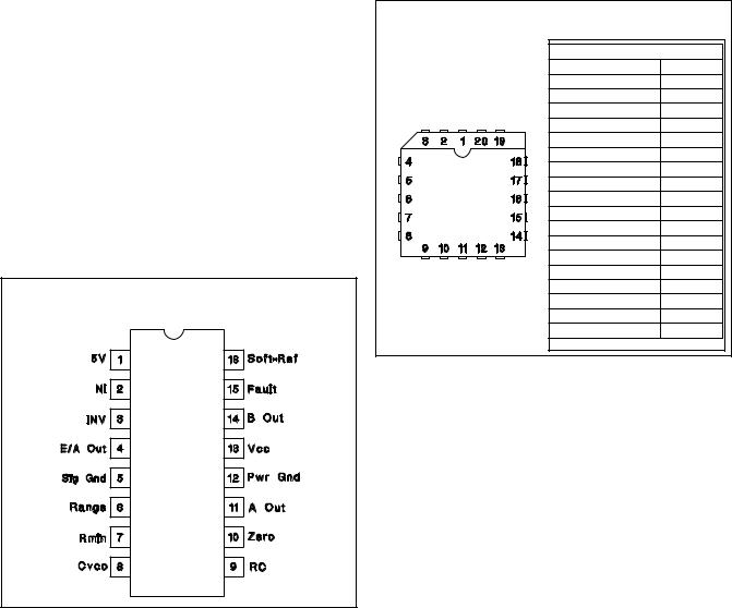
DIL-16, SOIC-16 (Top View)
J or N, DW Packages
CONNNECTION DIAGRAMS
PLCC-20 & LCC-20 (Top View) |
|
Q & L Package |
|
PACKAGE PIN FUNCTION |
|
FUNCTION |
PIN |
Soft Ref |
1 |
5V |
2 |
NI |
3 |
INV |
4 |
E/A Out |
5 |
Sig Gnd |
6 |
Range |
7 |
RMIN |
8 |
CVCO |
9 |
RC |
10 |
Zero |
11 |
NC |
12 |
NC |
13 |
A Out |
14 |
Pwr Gnd |
15 |
Pwr Gnd |
16 |
VCC |
17 |
B Out |
18 |
2
UC1861-1868
UC2861-2868
UC3861-3868
ELECTRICAL CHARACTERISTICS Unless otherwise stated, all specifications apply for –55°C≤TA≤125°C for the UC186x, –25°C≤TA≤85°C for the UC286x, and 0°C≤TA≤70°C for the UC386x, VCC=12V, CVCO=1nF, Range=7.15k, RMIN=86.6k, C=200pF, R=4.02k, and Csr=0.1μF. TA=TJ .
PARAMETER |
TEST CONDITIONS |
MIN |
TYP |
MAX |
UNITS |
5V Generator |
|
|
|
|
|
Output Voltage |
12V ≤ Vcc ≤ 20V, –10mA ≤ IO ≤ 0mA |
4.8 |
5.0 |
5.2 |
V |
Short Circuit Current |
VO = 0V |
–150 |
|
–15 |
mA |
Soft-Reference |
|
|
|
|
|
Restart Delay Current |
V = 2V |
10 |
20 |
35 |
μA |
Soft Start Current |
V = 2V |
–650 |
–500 |
–350 |
μA |
Reference Voltage |
TJ = 25°C, IO = 0A |
4.95 |
5.00 |
5.05 |
V |
|
12V ≤ VCC ≤ 20V, –200μA ≤ IO ≤ 200μA |
4.85 |
|
5.15 |
V |
Line Regulation |
12V ≤ VCC ≤ 20V |
|
2 |
20 |
mV |
Load Regulation |
–200μA ≤ IO ≤ 200μA |
|
10 |
30 |
mV |
Error Amplifier (Note 3) |
|
|
|
|
|
Input Offset Voltage |
VCM = 5V, Vo = 2V, IO = 0A |
–10 |
|
10 |
mV |
Input Bias Current |
VCM = 0V |
–2.0 |
–0.3 |
|
μA |
Voltage Gain |
Vcm = 5V, 0.5V ≤ VO ≤ 3.7V, IO = 0A |
70 |
100 |
|
dB |
Power Supply Rejection Ratio |
Vcm = 5V, VO = 2V, 12V ≤ VCC ≤ 20V |
70 |
100 |
|
dB |
Error Amplifier (Note 3) (cont.) |
|
|
|
|
|
Common Mode Rejection Ratio |
0V ≤ Vcm ≤ 6V, VO = 2V |
65 |
100 |
|
dB |
VOUT Low |
VID = –100mV, IO = 200μA |
|
0.17 |
0.25 |
V |
VOUT High |
VID = 100mV, IO = –200μA |
3.9 |
4.2 |
|
V |
Unity Gain Bandwidth |
(Note 4) |
0.5 |
0.8 |
|
MHz |
Voltage Controlled Oscillator |
|
|
|
|
|
Maximum Frequency |
VID (Error Amp) = 100mV, TJ = 25°C |
450 |
500 |
550 |
kHz |
|
VID (Error Amp) = 100mV |
425 |
|
575 |
kHz |
Minimum Frequency |
VID (Error Amp) = –100mV, TJ = 25°C |
45 |
50 |
55 |
kHz |
|
VID (Error Amp) = –100mV |
42 |
|
58 |
kHz |
One Shot |
|
|
|
|
|
Zero Comparator Vth |
|
0.45 |
0.50 |
0.55 |
V |
Propagation Delay |
(Note 4) |
|
120 |
200 |
ns |
Maximum Pulse Width |
VZERO = 1V |
850 |
1000 |
1150 |
ns |
Maximum to Minimum Pulse |
VZERO = 0V UCx861 – UCx864 |
2.5 |
4 |
5.5 |
|
Width Ratio |
VZERO = 0V UCx865 – UCx868. –55°C to +85°C |
4 |
5.5 |
7 |
|
|
VZERO = 0V UCx865 – UCx868, +125°C |
3.8 |
5.5 |
7 |
|
Output Stage |
|
|
|
|
|
Rise and Fall Time |
CLOAD = 1nF (Note 4) |
|
25 |
45 |
ns |
Output Low Saturation |
IO = 20mA |
|
0.2 |
0.5 |
V |
|
IO = 200mA |
|
0.5 |
2.2 |
V |
Output High Saturation |
IO = –200mA, down from Vcc |
|
1.7 |
2.5 |
V |
UVLO Low Saturation |
IO = 20mA |
|
0.8 |
1.5 |
V |
Fault Comparator |
|
|
|
|
|
Fault Comparator Vth |
|
2.85 |
3.00 |
3.15 |
V |
Delay to Output |
(Note 4) (Note 5) |
|
100 |
200 |
ns |
3
 Loading...