


 Loading...
TEXAS INSTRUMENTS UC1842, UC1843, UC1844, UC1845, UC2842 Technical data
...UC1842/3/4/5
UC2842/3/4/5
UC3842/3/4/5
www.ti.com |
SLUS223C – APRIL 1997 – REVISED JUNE 2007 |
|
CURRENT MODE PWM CONTROLLER
FEATURES
∙Optimized For Off-line and DC-to-DC Converters
∙Low Start-Up Current (<1 mA)
∙Automatic Feed Forward Compensation
∙Pulse-by-Pulse Current Limiting
∙Enhanced Load Response Characteristics
∙Under-Voltage Lockout With Hysteresis
∙Double Pulse Suppression
∙High Current Totem Pole Output
∙Internally Trimmed Bandgap Reference
∙500-kHz Operation
∙Low RO Error Amp
DESCRIPTION
The UC1842/3/4/5 family of control devices provides the necessary features to implement off-line or dc-to-dc fixed frequency current mode control schemes with a minimal external parts count. Internally implemented circuits include under-voltage lockout featuring start up current less than 1 mA, a precision reference trimmed for accuracy at the error amp input, logic to insure latched operation, a PWM comparator which also provides current limit control, and a totem pole output stage designed to source or sink high peak current. The output stage, suitable for driving N-Channel MOSFETs, is low in the off state.
Differences between members of this family are the under-voltage lockout thresholds and maximum duty cycle ranges. The UC1842 and UC1844 have UVLO
thresholds of 16 VON and 10 VOFF, ideally suited to off-line applications. The corresponding thresholds
for the UC1843 and UC1845 are 8.4 V and 7.6 V. The UC1842 and UC1843 can operate to duty cycles approaching 100%. A range of zero to 50% is obtained by the UC1844 and UC1845 by the addition of an internal toggle flip flop which blanks the output off every other clock cycle.
BLOCK DIAGRAM
Vcc |
7 12 |
|
|
|
|
|
|
|
|
UVLO |
|
|
|
|
|
|
34 V |
5 V |
|
|
|
|
|
S/R |
|
|
|
|
|
|
REF |
|
|
|
GROUND |
5 |
9 |
|
|
|
|
|
|
|
|
|||
|
|
|
2.50 V |
|
|
|
|
|
|
VREF |
|
Internal |
|
|
|
|
|
|
BIAS |
|
|
|
|
Good |
|
|
|
|
|
|
Logic |
|
|
|
RT/CT |
4 |
7 |
OSC |
|
|
|
|
|
|
|
|
T |
|
|
|
|
Error |
|
|
|
|
|
|
|
|
|
|
|
|
|
Amp |
|
S |
|
|
|
|
2R |
|
|
|
VFB |
2 |
3 |
R |
|
R |
PWM |
|
|
|||||
|
|
|
|
1 V |
CURRENT |
LATCH |
COMP |
1 |
1 |
|
|
||
|
|
SENSE |
|
|||
|
|
|
|
|
|
|
CURRENT |
3 |
5 |
|
|
COMPARATOR |
|
|
|
|
|
|||
SENSE |
|
|
|
|
||
|
|
|
|
|
|
|
Note 1: A/B |
A = DIL−8 Pin Number . B = SO−14 and CFP−14 Pin Number . |
|
||||
Note 2: |
Toggle flip flop used only in 1844 and 1845. |
|
|
|
||
8 14
14
VREF
5 V
50 mA
 7
7 11
11
VC

 6
6 10 OUTPUT
 5
5 8
8
POWER
GROUND
Please be aware that an important notice concerning availability, standard warranty, and use in critical applications of Texas Instruments semiconductor products and disclaimers thereto appears at the end of this data sheet.
PRODUCTION DATA information is current as of publication date. |
Copyright © 1997–2007, Texas Instruments Incorporated |
Products conform to specifications per the terms of the Texas |
|
Instruments standard warranty. Production processing does not |
|
necessarily include testing of all parameters. |
|

UC1842/3/4/5
UC2842/3/4/5
UC3842/3/4/5
SLUS223C – APRIL 1997 – REVISED JUNE 2007 |
www.ti.com |
||
|
|||
ABSOLUTE MAXIMUM RATINGS(1) |
|
||
|
|
UNIT |
|
Supply voltage |
Low impedance source |
30 V |
|
ICC < 30 mA |
Self Limiting |
||
|
|||
Output current |
|
±1 A |
|
Output energy (capacitive load) |
|
5 μJ |
|
Analog inputs (Pins 2, 3) |
|
–0.3 V to 6.3 V |
|
Error amp output sink current |
|
10 mA |
|
|
TA≤ 25°C (DIL-8) |
1 W |
|
Power dissipation |
TA≤ 25°C (SOIC-14) |
725 mW |
|
|
TA≤ 25°C (SOIC-8) |
650 mW |
|
Storage temperature range |
|
–65°C to 150°C |
|
Junction temperature range |
|
–55°C to 150°C |
|
Lead temperature (soldering, 10 seconds) |
300°C |
||
(1)All voltages are with respect to Pin 5. All currents are positive into the specified terminal. Consult Packaging Section of Databook for thermal limitations and considerations of packages.
CONNECTION DIAGRAMS
DIL-8, SOIC-8
N or J PACKAGE, D8 PACKAGE (TOP VIEW)
COMP |
|
|
|
|
|
VREF |
|
1 |
|
8 |
|
||
|
|
|
||||
VFB |
|
2 |
|
7 |
|
VCC |
|
|
|
||||
ISENSE |
|
3 |
|
6 |
|
OUTPUT |
|
|
|
||||
|
|
|
|
|
|
|
RT/CT |
|
4 |
|
5 |
|
GROUND |
|
|
|
|
|
|
|
|
|
|
|
|
|
|
SOIC-14, CFP-14 D or W PACKAGE (TOP VIEW)
COMP |
|
|
1 |
14 |
|
|
VREF |
|
|
|
|
||||
|
|
|
|
||||
NC |
|
|
2 |
13 |
|
|
NC |
|
|
|
|
||||
VFB |
|
3 |
12 |
|
|
VCC |
|
|
|
|
|
||||
|
|
|
|
||||
NC |
|
|
4 |
11 |
|
|
VC |
|
|
|
|
||||
ISENSE |
|
|
5 |
10 |
|
|
OUTPUT |
|
|
|
|
||||
NC |
|
|
6 |
9 |
|
|
GROUND |
|
|
|
|
||||
RT/CT |
|
7 |
8 |
|
|
PWR GND |
|
|
|
|
|
||||
|
|
|
|
||||
|
|
PLCC-20 |
|
||
|
|
Q PACKAGE |
|
||
|
NC |
(TOP VIEW) |
|
||
|
COMP |
NC |
V NC |
|
|
|
|
|
|
REF |
|
|
3 |
2 |
1 |
20 19 |
|
NC |
4 |
|
|
18 |
VCC |
VFB |
5 |
|
|
17 |
VC |
NC |
6 |
|
|
16 |
NC |
ISENSE |
7 |
|
|
15 |
OUTPUT |
NC |
8 |
|
|
14 |
NC |
|
9 |
10 11 12 13 |
|
||
NC |
R NC |
PWRGND |
GROUND |
|
T |
|
|
|
C / |
|
|
|
T |
|
|
NC − No internal connection
2 |
Submit Documentation Feedback |

|
|
|
UC1842/3/4/5 |
|
|
|
UC2842/3/4/5 |
www.ti.com |
|
|
UC3842/3/4/5 |
|
SLUS223C – APRIL 1997 – REVISED JUNE 2007 |
||
|
|
||
THERMAL CHARACTERISTICS |
|
|
|
over operating free-air temperature range (unless otherwise noted) |
|
|
|
PACKAGE |
|
θJC |
θJA |
DIL-8 |
J |
28(1) |
125-160 |
|
N |
25 |
110(2) |
SOIC-8 |
D8 |
42 |
84-160(2) |
SOIC-14 |
D14 |
35 |
50-120(2) |
CFP-14 |
W |
5.49°C/W |
175.4C/W |
PLCC-20 |
Q |
34 |
43-75(2) |
(1)θJC data values stated were derived from MIL-STD-1835B.
(2)Specified θJA (junction to ambient) is for devices mounted to 5 in2 FR4 PC board with one ounce copper where noted. When resistance range is given, lower values are for 5 in2. Test PWB was 0.062 in thick and typically used 0.635-mm trace widths for power packages and 1.3-mm trace widths for non-power packages with 100 x 100-mil probe land area at the end of each trace.
DISSIPATION RATINGS
PACKAGE |
TA≤ 25°C |
DERATING FACTOR |
TA≤ 70°C |
TA≤ 85°CPO |
TA≤ 125°C |
|
POWER RATING |
ABOVE TA≤ 25°C |
POWER RATING |
WER RATING |
POWER RATING |
W |
700 mW |
5.5 mW/°C |
452 mW |
370 mW |
150 mW |
ELECTRICAL CHARACTERISTICS
Unless otherwise stated, these specifications apply for –55°C ≤ TA≤ 125°C for the UC184X; –40°C ≤ TA≤ 85°C for the UC284X; 0°C ≤ TA≤ 70°C for the 384X; VCC = 15 V(1); RT = 10 kΩ; CT = 3.3 nF, TA = TJ.
|
|
|
UC1842/3/4/5 |
|
UC3842/3/4/5 |
|
|
||
PARAMETER |
|
TEST CONDITIONS |
UC2842/3/4/5 |
|
|
UNIT |
|||
|
|
|
|
|
|||||
|
|
|
MIN |
TYP |
MAX |
MIN |
TYP |
MAX |
|
REFERENCE SECTION |
|
|
|
|
|
|
|
|
|
Output Voltage |
TJ = 25°C, IO = 1 mA |
4.95 |
5.00 |
5.05 |
4.90 |
5.00 |
5.10 |
V |
|
Line Regulation |
12 ≤ VIN≤ 25 V |
|
6 |
20 |
|
6 |
20 |
mV |
|
Load Regulation |
1 ≤ I0≤ 20 mA |
|
6 |
25 |
|
6 |
25 |
||
|
|
|
|||||||
Temp. Stability |
See (2)(3) |
|
0.2 |
0.4 |
|
0.2 |
0.4 |
mV/°C |
|
Total Output Variation |
Line, load, tempature (2) |
4.9 |
|
5.1 |
4.82 |
|
5.18 |
V |
|
Output Noise Voltage |
10 Hz≤ f ≤ 10 kHz, T = 25°C(2) |
|
50 |
|
|
50 |
|
μV |
|
|
|
J |
|
|
|
|
|
|
|
Long Term Stability |
T = 125°C, 1000 Hrs(2) |
|
5 |
25 |
|
5 |
25 |
mV |
|
|
A |
|
|
|
|
|
|
|
|
Output Short Circuit |
|
|
–30 |
–100 |
–180 |
–30 |
–100 |
–180 |
mA |
OSCILLATOR SECTION |
|
|
|
|
|
|
|
|
|
Initial Accuracy |
T |
= 25°C(4) |
47 |
52 |
57 |
47 |
52 |
57 |
kHz |
|
J |
|
|
|
|
|
|
|
|
Voltage Stability |
12 ≤ VCC≤ 25 V |
|
0.2% |
1% |
|
0.2% |
1% |
|
|
Temp. Stability |
TMIN≤ TA≤ TMAX (2) |
|
5% |
|
|
5% |
|
|
|
Amplitude |
V |
4 peak-to-peak (2) |
|
1.7 |
|
|
1.7 |
|
V |
|
PIN |
|
|
|
|
|
|
|
|
(1)Adjust VCC above the start threshold before setting at 15 V.
(2)These parameters, although specified, are not 100% tested in production.
(3)Temperature stability, sometimes referred to as average temperature coefficient, is described by the equation:
VREF(max) *VREF (min) |
|
||
Temp Stability + |
|
|
|
TJ(max) * TJ (min) |
VREF(max) and VREF(min) are the maximum and minimum reference voltages measured over |
||
|
|
|
|
the appropriate temperature range. Note that the extremes in voltage do not necessarily occur at the extremes in temperature. |
|||
(4)Output frequency equals oscillator frequency for the UC1842 and UC1843. Output frequency is one half oscillator frequency for the UC1844 and UC1845.
Submit Documentation Feedback |
3 |

UC1842/3/4/5
UC2842/3/4/5
UC3842/3/4/5
www.ti.com
SLUS223C – APRIL 1997 – REVISED JUNE 2007
ELECTRICAL CHARACTERISTICS (continued)
Unless otherwise stated, these specifications apply for –55°C ≤ TA≤ 125°C for the UC184X; –40°C ≤ TA≤ 85°C for the UC284X; 0°C ≤ TA≤ 70°C for the 384X; VCC = 15 V; RT = 10 kΩ; CT = 3.3 nF, TA = TJ.
|
|
UC1842/3/4/5 |
UC3842/3/4/5 |
|||
PARAMETER |
TEST CONDITIONS |
UC2842/3/4/5 |
||||
|
UNIT |
|||||
|
|
MIN |
TYP MAX |
MIN |
TYP MAX |
|
ERROR AMP SECTION
 Input Voltage
Input Bias Current
AVOL
 Unity Gain Bandwidth
PSRR
 Output Sink Current
Output Source Current
 VOUT High
VOUT Low
 CURRENT SENSE SECTION
Gain
 Maximum Input Signal
PSRR
 Input Bias Current
Delay to Output
OUTPUT SECTION
VPIN 1 |
= 2.5 V |
2.45 |
2.50 |
2.55 |
2.42 |
2.50 |
2.58 |
V |
|
|
|
|
|
–0.3 |
–1 |
|
–0.3 |
–2 |
μA |
2 ≤ VO≤ 4 V |
65 |
90 |
|
65 |
90 |
|
dB |
||
T = 25°C (5) |
0.7 |
1 |
|
0.7 |
1 |
|
MHz |
||
J |
|
|
|
|
|
|
|
|
|
12 ≤ VCC≤ 25 V |
60 |
70 |
|
60 |
70 |
|
dB |
||
VPIN 2 |
= 2.7 V, VPIN 1 = 1.1 V |
2 |
6 |
|
2 |
6 |
|
mA |
|
VPIN 2 |
= 2.3 V, VPIN 1 = 5 V |
–0.5 |
–0.8 |
|
–0.5 |
–0.8 |
|
||
|
|
|
|||||||
VPIN 2 |
= 2.3 V, RL = 15 kΩ to ground |
5 |
6 |
|
5 |
6 |
|
V |
|
VPIN 2 |
= 2.7 V, RL = 15 kΩ to Pin 8 |
|
0.7 |
1.1 |
|
0.7 |
1.1 |
||
|
|
|
|||||||
See (6)(7) |
2.85 |
3 |
3.15 |
2.85 |
3 |
3.15 |
V/V |
||
V |
= 5 V (6) |
0.9 |
1 |
1.1 |
0.9 |
1 |
1.1 |
V |
|
PIN 1 |
|
|
|
|
|
|
|
|
|
12 ≤ V |
CC |
≤ 25 V (5)(6) |
|
70 |
|
|
70 |
|
dB |
|
|
|
|
|
|
|
|
|
|
|
|
|
|
–2 |
–10 |
|
–2 |
–10 |
μA |
V |
= 0 V to 2 V (5) |
|
150 |
300 |
|
150 |
300 |
ns |
|
PIN 3 |
|
|
|
|
|
|
|
|
|
Output Low Level |
ISINK = 20 mA |
|
|
0.1 |
0.4 |
|
0.1 |
0.4 |
|||
ISINK = 200 mA |
|
1.5 |
2.2 |
|
1.5 |
2.2 |
|||||
|
|
|
|||||||||
|
ISOURCE = 20 mA |
13 |
13.5 |
|
13 |
13.5 |
V |
||||
Output High Level |
|
|
|||||||||
ISOURCE = 200 mA |
12 |
13.5 |
|
12 |
13.5 |
|
|||||
|
|
|
|||||||||
Rise Time |
T |
J |
= 25°C, C |
L |
= 1 nF (5) |
|
50 |
150 |
|
50 |
150 |
|
|
|
|
|
|
|
|
|
ns |
||
Fall Time |
T |
|
= 25°C, C |
|
= 1nF(5) |
|
50 |
150 |
|
50 |
|
J |
L |
|
|
150 |
|||||||
UNDER-VOLTAGE LOCKOUT SECTION |
|
|
|
|
|
|
|
|
|||
Start Threshold |
X842/4 |
|
|
15 |
16 |
17 |
14.5 |
16 |
17.5 |
||
X843/5 |
|
|
7.8 |
8.4 |
9.0 |
7.8 |
8.4 |
9.0 |
|||
|
|
|
|||||||||
|
|
|
|
|
|
|
|
|
|
|
V |
Min. Operating Voltage After |
X842/4 |
|
|
9 |
10 |
11 |
8.5 |
10 |
11.5 |
||
Turn On |
X843/5 |
|
|
7.0 |
7.6 |
8.2 |
7.0 |
7.6 |
8.2 |
||
PWM SECTION |
|
|
|
|
|
|
|
|
|
|
|
Maximum Duty Cycle |
X842/3 |
|
|
95% |
97% |
100% |
95% |
97% |
100% |
||
X844/5 |
|
|
46% |
48% |
50% |
47% |
48% |
50% |
|||
|
|
|
|||||||||
Minimum Duty Cycle |
|
|
|
|
|
|
|
0% |
|
|
0% |
TOTAL STANDBY CURRENT |
|
|
|
|
|
|
|
|
|
|
|
Start-Up Current |
|
|
|
|
|
|
0.5 |
1 |
|
0.5 |
1 |
|
VPIN 2 = VPIN 3 = 0 V |
|
|
|
|
|
mA |
||||
Operating Supply Current |
|
11 |
17 |
|
11 |
17 |
|||||
VCC Zener Voltager |
ICC = 25 mA |
|
|
30 |
34 |
|
30 |
34 |
V |
||
(5)These parameters, although specified, are not 100% tested in production.
(6)Parameter measured at trip point of latch with VPIN 2 = 0.
(7) Gain defined as: |
A + DVPIN 1 |
, 0 v VPIN 3 v 0.8 V |
DVPIN 3 |
|
4 |
Submit Documentation Feedback |
UC1842/3/4/5 UC2842/3/4/5
UC3842/3/4/5
www.ti.com
SLUS223C – APRIL 1997 – REVISED JUNE 2007
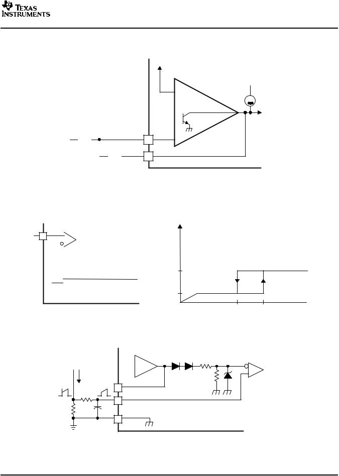
ERROR AMP CONFIGURATION
Error amp can source or sink up to 0.5 mA.
2.5 V
0.5 mA
+
|
|
|
|
|
VFB |
|
_ |
|
ZI |
|
|
|
2 |
||
|
|
|
|
||||
|
|
|
|
|
COMP |
|
|
|
|
|
|
ZF |
|
1 |
|
|
|
|
|
|
|||
UNDER-VOLTAGE LOCKOUT
During under-voltage lock-out, the output drive is biased to sink minor amounts of current. Pin 6 should be shunted to ground with a bleeder resistor to prevent activating the power switch with extraneous leakage currents.
VCC
VCC |
7 |
|
|
|
|
|
|
|
|
|
ON/OFF Command |
|
|||
|
|
|
|
|
|
|
|
|
|
|
|
to REST of IC |
|
||
|
|
|
|
|
|
|
|
|
|
|
|
|
|
|
|
|
|
|
|
|
|
|
|
|
|
|
UC1842 |
UC1843 |
|
<17 mA |
|
|
|
|
|
|
|
|
|
|
|
|
UC1844 |
UC1845 |
|
||
|
|
|
|
|
|
|
|
|
|
|
|
|
|||
|
|
|
|
|
|
VON |
|
16 V |
8.4 V |
|
|
||||
|
|
|
|
|
|||||||||||
|
|
|
|
VOFF |
|
10 V |
7.6 V |
|
<1 mA |
||||||
 VCC
VCC
VOFF VON
CURRENT SENSE CIRCUIT
A small RC filter may be required to suppress switch transients.
|
|
ERROR |
|
|
|
AMP |
2R |
|
|
|
|
IS |
|
|
R |
|
1 |
COMP |
1 V CURRENT |
|
|
SENSE |
|
R |
|
CURRENT |
COMPARATOR |
|
3 |
|
|
|
SENSE |
|
|
C |
|
|
|
|
|
|
|
RS |
5 |
GND |
|
|
|
|
|
5 |
|
|
|
|
Peak Current (IS) is Determined By The Formula |
||
|
|
ISMAX |
,1.0 V |
|
|
RS |
|
|
|
|
|
Submit Documentation Feedback |
5 |

UC1842/3/4/5
UC2842/3/4/5
UC3842/3/4/5
www.ti.com
SLUS223C – APRIL 1997 – REVISED JUNE 2007
OSCILLATOR SECTION
VREF 8
RT
RT/CT 4
CT
GROUND 5
1.72 For RT> 5 K f ~ RTCT
td − ms
Deadtime vs CT (RT >5 kW) |
Timing Resistance vs Frequency |
30 |
|
|
|
|
|
|
|
100 |
|
|
|
|
|
|
|
|
|
|
|
|
|
|
|
|
|
10 |
|
|
|
|
|
|
|
30 |
|
|
|
|
|
|
|
|
|
|
|
W) |
|
|
|
|
|
|
|
|
|
|
|
|
|
|
|
|
|
|
3 |
|
|
|
|
|
|
(k |
|
|
|
|
|
|
|
|
|
|
|
|
− |
|
|
|
|
|
|
|
|
|
|
|
|
T |
10 |
|
|
|
|
1 |
|
|
|
|
|
|
R |
|
|
|
|
|
|
|
|
|
|
|
|
|
|
|
|
|
|
0.3 |
|
|
|
|
|
|
|
3 |
|
|
|
|
1 |
2.2 |
4.7 |
10 |
22 |
47 |
100 |
|
100 |
1 k |
10 k |
100 k |
1 M |
|
|
|
CT − nF |
|
|
|
|
|
f − Frequency − Hz |
|
||
OUTPUT SATURATION CHARACTERISTICS
Saturation Voltage − V
4 |
|
|
|
|
VCC = 15 V |
|
|
3 |
|
|
|
|
|
TA = 25°C |
|
|
TA = −55 °C |
|
|
2 |
|
|
|
1 |
|
SOURCE SAT |
|
|
(VCC − |
VOH) |
|
|
|
||
|
|
SINK SAT (VOL) |
|
0 |
|
|
|
.01 |
.02 .03 .04 .05 .07 .1 |
.2 .3 .4 |
.5 .7 1 |
Output Current, Source or Sink − A
ERROR AMPLIFIER OPEN-LOOP FREQUENCY RESPONSE
|
80 |
|
− dB |
60 |
|
θ |
||
VoltageGain |
||
20 |
||
|
40 |
|
|
Av |
|
|
0 |
0
−45
−90
−135
−180
Phase Margin − °
10 |
100 |
1 k |
10 k |
100 k |
1 M |
10 M |
f − Frequency − Hz
6 |
Submit Documentation Feedback |
UC1842/3/4/5 UC2842/3/4/5
UC3842/3/4/5
www.ti.com
SLUS223C – APRIL 1997 – REVISED JUNE 2007
OPEN-LOOP LABORATORY FIXTURE
High peak currents associated with capacitive loads necessitate careful grounding techniques. Timing and bypas capacitors should be conected close to pin 5 in a single point ground. The transistor and 5k potentiometer are used to sample the oscillator waveform and apply an adjustable ramp to pin 3.
|
|
|
|
|
|
|
VREF |
|
|
R1 |
|
|
|
|
|
|
2N2222 |
|
|
UC1842 |
|
A |
VCC |
4.7 kW |
100 kW |
|
|
|
|||
1 |
COMP |
VREF |
8 |
|
|
||
|
|
0.1 mF |
|
||||
1 kW |
|
2 |
VFB |
VCC |
7 |
|
|
ERROR AMP |
|
0.1 mF |
|
||||
ADJUST |
5 kW |
|
|
|
|
|
1 kW 1 W |
|
3 |
ISENSE |
OUTPUT |
6 |
|
||
|
I |
|
OUTPUT |
||||
4.7 kW |
SENSE |
|
|
|
|
|
|
ADJUST |
|
|
|
|
|
|
|
|
|
4 |
RT / CT |
GROUND |
5 |
|
|
|
|
|
|
CT |
|
|
GROUND |
|
|
|
|
|
|
|
SHUTDOWN TECHNIQUES
Shutdown of the UC1842 can be accomplished by two methods; either raise pin 3 above 1 V or pull pin 1 below a voltage two diode drops above ground. Either method causses the output of the PWM comparator to be high (refer to block diagram). The PWM latch is reset dominant so that the output will remain low until the next clock cycle after the shutdown condition at pin 1 and/or 3 is removed. In one example, an externally latched shutdown may be accomplished by adding an SCR which will be reset by cycling VCC below the lower UVLO threshold. At this pint the reference turns off, allowing the SCR to reset.
1 kW
8 VREF |
|
1 COMP |
|
SHUTDOWN
330 W |
3 |
ISENSE |
|
||
|
500 W |
|
SHUTDOWN |
|
|
|
To Current |
|
|
SENSE RESISTOR |
|
Submit Documentation Feedback |
7 |

UC1842/3/4/5 |
|
|
|
|
|
|
|
|
|
|
|
|
|
|
UC2842/3/4/5 |
|
|
|
|
|
|
|
|
|
|
|
|
|
|
UC3842/3/4/5 |
|
|
|
|
|
|
|
|
|
|
|
|
www.ti.com |
|
SLUS223C – APRIL 1997 – REVISED JUNE 2007 |
|
|
|
|
|
|
|
|
|
|
||||
|
|
|
|
|
|
|
|
|
|
|
||||
OFFLINE FLYBACK REGULATOR |
|
|
|
|
|
|
|
|
|
|
||||
R1 |
|
|
|
|
|
|
|
|
T1 |
|
D6 |
L1 |
|
|
|
|
|
|
|
|
|
|
|
U9D946 |
|
|
|
||
5 Ω 1 W |
|
|
|
|
|
|
|
|
|
|
|
|
||
|
|
|
|
|
|
|
|
|
|
|
|
|
+6 V |
|
|
|
|
|
|
|
|
|
|
|
|
|
|
|
|
117 VAC |
VARO |
|
|
|
|
R12 |
|
C9 |
|
N5 |
C10 |
|
C11 |
|
VM 68 |
C1 |
|
|
|
4.7 kΩ |
|
3300 pF |
|
µF |
|||||
|
|
|
|
|
4700 µF |
|
4700 |
|||||||
|
|
250 µF |
|
|
|
2 W |
|
600 V |
|
|
10 V |
|
10 V |
|
|
|
250 V |
|
|
|
|
|
NP |
|
|
|
|||
|
|
R2 |
|
|
|
|
|
|
|
|
|
COM |
||
|
|
|
56 kΩ |
|
|
|
|
D4 |
|
|
D7 |
|
|
|
|
|
|
2 W |
|
|
|
|
|
|
|
|
|
||
|
|
|
|
|
|
|
1N3613 |
|
|
|
|
|||
|
|
|
|
|
|
|
|
|
UF81002 |
|
|
|
||
|
|
|
|
|
|
|
|
|
|
|
|
|
|
|
|
|
|
|
|
|
|
|
|
|
|
|
|
|
+12 V |
|
|
|
|
|
|
D2 |
|
D3 |
|
|
|
C12 |
µF |
|
|
R4 |
R3 |
|
|
|
|
|
N12 |
|
2200 |
|
|||
|
|
|
|
1N3612 |
1N3612 |
|
16 V |
|
|
|||||
|
4.7 kΩ |
20 kΩ |
|
|
|
|
|
|
±12 V COM |
|||||
|
|
|
|
|
|
|
|
|
|
|
|
|||
|
|
|
|
|
|
|
|
|
|
N12 |
|
C13 |
|
|
|
|
|
|
|
|
|
|
|
|
|
|
µF |
|
|
|
|
|
|
C2 |
|
R9 |
C4 |
|
|
|
2200 |
|
||
|
|
|
|
C3 |
|
|
|
16 V |
|
|
||||
|
|
|
7 |
100 µF |
22 µF |
68 |
Ω |
47 µF |
|
|
|
|
|
|
|
|
2 |
25 V |
3 W |
25 V |
NC |
|
|
|
|
−12 V |
|||
|
|
R5 150 kΩ |
|
|
|
|
|
|
|
|
D8 |
|
|
|
|
|
1 |
|
|
|
|
|
|
|
|
|
|
|
|
|
|
|
|
|
|
|
|
|
|
UES1002 |
|
|
|
|
|
|
C14 |
|
|
|
|
|
|
|
|
|
|
|
|
|
|
UC3844 |
|
|
|
|
|
|
|
|
|
|
|
|
|
|
|
|
|
R7 |
|
|
|
|
|
|
|
||
|
|
100 pF |
|
|
|
|
Q1 |
|
|
|
|
|
||
|
|
|
|
|
22 Ω |
|
|
|
C8 |
|
|
|||
|
|
|
|
|
|
UFN833 |
|
|
|
|||||
|
|
8 |
6 |
|
|
|
|
|
|
680 pF |
|
|||
|
|
|
|
|
|
|
|
|
|
|
||||
|
|
R6 |
|
|
|
|
R8 |
|
|
|
|
600 V |
|
|
|
|
10 kΩ |
3 |
|
|
|
1 kΩ |
|
|
|
|
|
|
|
|
C5 |
4 |
5 |
|
USD1120 |
|
R10 |
|
|
|
|
|
||
|
µF |
|
|
|
|
|
|
|
|
|||||
|
0.01 |
|
|
|
|
C7 |
R13 |
Ω |
|
D8 |
|
R11 |
||
|
|
C6 |
|
|
|
|
0.55 |
|
|
2.7 kΩ |
||||
|
|
0.0022 µF |
|
|
|
|
470 pF |
20 kΩ |
1 W |
|
|
1N3613 |
||
|
|
|
|
|
|
|
|
|
|
|
|
2 W |
||
Power Supply Specifications
1.Input Voltages
a. 5VAC to 130VA (50 Hz/60 Hz)
2.Line Isolation: 3750 V
3.Switchng Frequency: 40 kHz
4.Efficiency at Full Load 70%
5.Output Voltage:
a.+5 V, ±5%; 1A to 4A load Ripple voltage: 50 mV P-P Max
b.+12 V, ±3%; 0.1A to 0.3A load Ripple voltage: 100 mV P-P Max
c.–12 V, ±3%; 0.1A to 0.3A load Ripple voltage: 100 mV P-P Max
SLOPE COMPENSATION
A fraction of the oscillator ramp can be resistively summed with the current sense signal to provide slope compensation for converters requiring duty cycles over 50%.
VREF 8
0.1 mF |
RT |
RT / CT 4
CT 
UC1842/3
R1 |
ISENSE |
R2
ISENSE 3
C
RSENSE
8 |
Submit Documentation Feedback |
Loading...