


UC1852

DESCRIPTION
The UC1852 provides a low-cost so lution to active power-f actor corr ection (PF C)
for systems that would otherwise draw high peak current pulses from AC power
lines. This circuit implements zero-current switched boost conversion, producing
sinusoidal input currents with a minimum of external components, while keeping
peak current substantially below that of fully-discontinuous convert ers.
The UC1852 provides controlled switch on-time to regulate the output bulk DC
voltage, an off-time defined by the boost inductor, and a zero-current sensing
circuit to reactivate the switch cycle. Even though switching frequency var ies with
both load and instantaneous line voltage, it can be maintained within a reasonable
range to minimize noise generation.
While allowing higher peak switch currents than continuous PFCs such as the
UC1854, this device offers less extern al circuitry and smaller inductors, yet better
performance and easier line-noise filtering than discontinuous current PFCs with
no sacrifice in complexity or c ost. The ability to obtain a power fact or in excess of
0.99 makes the UC1852 an optimum choice for low-cost applications in the 50 to
500 watt power range. Protect ion features of these devices include under-v oltage
lockout, output clamping, peak-current limiting, and maximum-frequency
clamping.
The UC1852 family is available in 8-pin plastic and ceramic dual in-line packages,
and in the 8-pin small outline IC package (SOIC). The UC1852 is specified for
operation from -55°C to +125°C, the UC2852 is specified for operation from -40°C
to +85°C, and the UC3852 is specified for operation from 0°C to +70° C.
UC1852
UC2852
UC3852
查询UC1852供应商
High Power-Factor Preregulato r
FEATURES
Low-Cost Power Factor
•
Correction
• Power Factor Greater Than 0.99
• Few External Parts Required
• Controlled On-Time Boost PWM
• Zero-Current Switching
• Limited Peak Current
• Min and Max Frequency Limits
• Starting Current Less Than 1mA
• High-Current FET Drive Output
• Under-Voltage Lockout
TYPICAL APPLICATION
10/94
UDG-92001
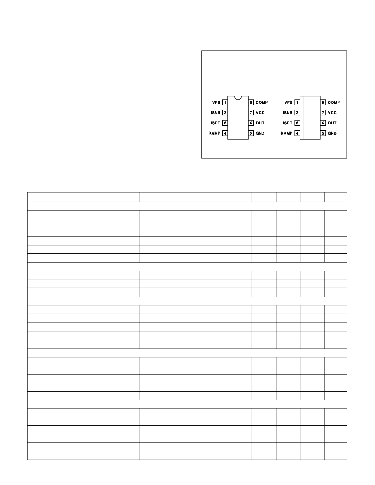
SOIC–8 (TOP VIEW)
D Package
Unless otherwise stated, VCC=2 4V, ISET=50k Ω to GND, RAMP=1nF to GND, ISNS=
–0.1V, VFB conne cted to COM P, no load on OU T, –5 5 °C<Ta<+125°C for the UC1852,
–40°C<Ta<+85°C f or the UC2852, and 0 °C<Ta<+70°C for the UC3852, and Ta=Tj.
ABSOLUTE MAXIMUM RATINGS
Supply Voltage (Lo w-im peda nce Sou rce )..........................30.0V
Supply Current (High-impedance Source)......................30.0mA
OUT Current, Peak.................. .... .... .... .... .... ... .... .... .... .... ....±1.0A
OUT Energy, Capacitive Load................ .... .... .... .... ..... .... ...5.0 µJ
Input Voltage, ISNS............................................................±5.0V
Input Voltage, VFB.............................................–0.3V to +10.0V
COMP Current...............................................................±10.0mA
ISET Current............ .... ... .... .... . .... ... .... .... . .... ... .... .... . .... ..–10.0mA
Power Dissipation at T a≤25°C (Note 3) ..............................1.0W
Storage Temperature .......................................–65°C to +150°C
Lead Temperat ur e (Soldering, 10 Sec onds )...................+300°C
CONNECTION DIAG RAM
Note 1: All voltages with respe ct to GND (Pin 1).
Note 2: All current s are posit iv e into the specif ied term inal.
Note 3: Refers to DIL-8 Packa ge. Consu lt Packaging Sec tion of
Unitrode Inte gra ted C ircuit s datab ook f or thermal lim ita tion s and
consideratio ns of package.
ELECTRICAL CHARACTERIST ICS
PARAMETER TEST CONDITIONS MIN. TYP. MAX. UNITS
Timer Sectio n
ISET Voltage 4.5 5.0 5.5 V
RAMP Charge Current RAMP=2.5V 88 98 108
RAMP Discharge Current ISNS= –1.0V, RAMP= 1 .0V 12 28 50 mA
RAMP Saturation Volt age
RAMP Threshold - Maximum Fre quen cy VFB=10V, COMP open 0.92 1.02 1.12 V
RAMP Threshold - PWM Comp ara tor 3.9 4.3 4.8 V
Current Sense Co mparator
ISNS Restart Threshold –18 –10 –4 mV
ISNS Fault Thres hold –550 –45 0 –350 mV
ISNS Input Current –100 –30 100
Error Amplifier Se cti o n
VFB Input Voltage 4.6 5.0 5.3 V
VFB Input Bias Current –5.00 –0.03 5.00
COMP Sink Current COMP=7.5V 10 mA
COMP Source Current COMP=2.5V –300 –175 –100
COMP Clamp Voltage VFB=0.0V, COMP open 9.2 10.0 10.6 V
OUT Output
OUT Saturation Voltag e High VCC=13V, I
OUT Saturation Voltag e Lo w I
OUT Saturation Voltag e Low @ 10m A I
OUT Clamp Voltage I
OUT Voltage during UVLO I
Overall Secti on
Inactive Supply Current VCC=10V 0.2 0.4 1.0 mA
Active Supply Current 3.0 6.0 10.0 mA
VCC Clamp Voltage ICC=25mA 30 33 36 V
VCC Turn-On Threshold 14.5 16.3 17.5 V
VCC Turn-Off Threshold 10.5 11.5 13.0 V
VCC Threshold Hysteresis 3 5 7 V
ISNS= –1.0V, I
OUT=200mA, ISNS= –1.0V 0.5 1.6 2.2 V
OUT=10mA, ISNS= –1.0V 0.05 0.40 V
OUT= –200mA, RAMP=2V 10.0 12.0 14.5 V
OUT=100mA, VCC=0V 0.5 1.0 2.2 V
RAMP=100µA
OUT= –200mA, RAMP=2V 0.5 1.7 2.5 V
2
UC1852
UC2852
UC3852
DIL–8 (TOP VIEW)
J or N Package
UDG-92002
µA
0.006 0.200 V
µA
µA
µA
 Loading...