


Texas Instruments UC3524ADW, UC3524AN, UC3524ADWTR, UC2524AN, UC2524ADWTR Datasheet
...
UC1524A
UC2524A
UC3524A
Advanced Regulating Pulse Width Modulators
FEATURES
•Fully Interchangeable with Standard UC1524 Family
•Precision Reference Internally Trimmed to ±1%
•High-Performance Current Limit Function
•Under-Voltage Lockout with Hysteretic Turn-on
•Start-Up Supply Current Less Than 4mA
•Output Current to 200mA
•60V Output Capability
•Wide Common-Mode Input Range for both Error and Current Limit Amplifiers
•PWM Latch Insures Single Pulse per Period
•Double Pulse Suppression Logic
•200ns Shutdown through PWM Latch
•Guaranteed Frequency Accuracy
•Thermal Shutdown Protection
BLOCK DIAGRAM
DESCRIPTION
The UC1524A family of regulating PWM ICs has been designed to retain the same highly versatile architecture of the industry standard UC1524 (SG1524) while offering substantial improvements to many of its limitations. The UC1524A is pin compatible with “non-A” models and in most existing applications can be directly interchanged with no effect on power supply performance. Using the UC1524A, however, frees the designer from many concerns which typically had required additional circuitry to solve.
The UC1524A includes a precise 5V reference trimmed to ±1% accuracy, eliminating the need for potentiometer adjustments; an error amplifier with an input range which includes 5V, eliminating the need for a reference divider; a current sense amplifier useful in either the ground or power supply output lines; and a pair of 60V, 200mA uncommitted transistor switches which greatly enhance output versatility.
An additional feature of the UC1524A is an under-voltage lockout circuit which disables all the internal circuitry, except the reference, until the input voltage has risen to 8V. This holds standby current low until turn-on, greatly simplifying the design of low power, off-line supplies. The turn-on circuit has approximately 600mV of hysteresis for jitter-free activation.
Other product enhancements included in the UC1524A’s design include a PWM latch which insures freedom from multiple pulsing within a period, even in noisy environments, logic to eliminate double pulsing on a single output, a 200ns external shutdown capability, and automatic thermal protection from excessive chip temperature. The oscillator circuit of the UC1524A is usable beyond 500kHz and is now easier to synchronize with an external clock pulse.
The UC1524A is packaged in a hermetic 16-pin DIP and is rated for operation from -55°C to +125°C. The UC2524A and 3524A are available in either ceramic or plastic packages and are rated for operation from -25°C to +85°C and 0°C to 70°C, respectively. Surface mount devices are also available.
VIN |
15 |
|
|
|
|
|
|
|
|
|
|
|
|
|
OSC |
3 |
|
RT |
|
|
|
|
|
|
||
6 |
||
CT |
|
|
7 |
||
COMP |
|
|
|
|
|
|
||
|
|
|
9 |
||
INV. INPUT |
|
|
|
|
|
1 |
||
N.I. INPUT |
|
|
|
|
|
|
||
2 |
||
CL (+) SENSE |
|
|
|
|
|
|
||
4 |
||
CL (–) SENSE |
|
|
|
|
|
|
||
5 |
||
|
|
|
|
|
|
|
+5V |
|
|
|
|
REFERENCE |
|
U.V. |
POWER TO |
REGULATOR |
|
|
|
|||
|
|
INTERNAL |
|
|
|
SENSE |
|
|
|
|
CIRCUITRY |
|
||
|
|
FLIP |
||
|
|
|
|
|
|
|
|
|
FLOP |
|
|
|
|
T |
OSC |
CLOCK |
|
|
|
|
|
|
|
|
|
RAMP |
COMP |
R |
|
|
|
S |
PWM |
|
|
|
S |
|
|
|
VIN |
LATCH |
|
|
|
|
|
|
|
|
E/A |
|
|
1k |
200mV |
VIN |
6V |
10k |
5.5V |
+ |
|
|||
|
|
|
|
|
|
C/L |
|
|
|
16 VREF
12 CA
11 EA
13CB
14EB
10 SHUTDOWN
8 GND
UDG-99178
SLUS181A - NOVEMBER 1999
ABSOLUTE MAXIMUM RATINGS
Supply Voltage (VIN) . . . . . . . . . . . . . . . . . . . . . . . . . . . . . . 40V Collector Supply Voltage (VC) . . . . . . . . . . . . . . . . . . . . . . . 60V Output Current (each Output). . . . . . . . . . . . . . . . . . . . . 200mA Maximum Forced Voltage (Pin 9, 10) . . . . . . . . . . . . . -3 to +5V Maximum Forced Current (Pin 9, 10) . . . . . . . . . . . . . . . ±10mA Reference Output Current . . . . . . . . . . . . . . . . . . . . . . . . 50mA Oscillator Charging Current . . . . . . . . . . . . . . . . . . . . . . . . 5mA Power Dissipation at TA = +25°C. . . . . . . . . . . . . . . . . 1000mW Power Dissipation at TC = +25°C . . . . . . . . . . . . . . . . 2000mW Operating Temperature Range . . . . . . . . . . . . -55°C to +125°C Storage Temperature Range. . . . . . . . . . . . . . -65°C to +150°C Lead Temperature, (Soldering, 10 seconds) . . . . . . . . . +300°C
Note: Consult packaging section of Databook for thermal limitations and considerations of package.
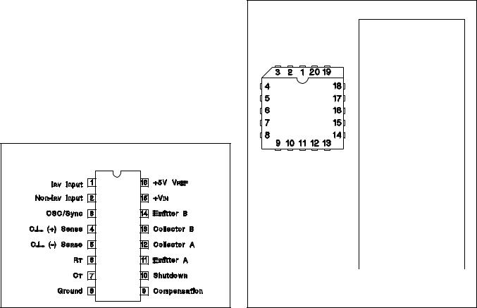
DIL-16, SOIC-16 (TOP VIEW)
J or N Package, DW Package
UC1524A
UC2524A
UC3524A
CONNECTION DIAGRAMS
PLCC-20, LCC-20 (TOP VIEW)
Q or L Package
PACKAGE PIN FUNCTION
FUNCTION |
PIN |
N/C |
1 |
Inv. Input |
2 |
Non-Inv. Input |
3 |
OSC/SYNC |
4 |
C.L. (+) sense |
5 |
N/C |
6 |
C.L. (-) sense |
7 |
RT |
8 |
CT |
9 |
Ground |
10 |
N/C |
11 |
Compensation |
12 |
Shutdown |
13 |
Emitter A |
14 |
Collector A |
15 |
N/C |
16 |
Collector B |
17 |
Emitter B |
18 |
+VIN |
19 |
+5V VREF |
20 |
ELECTRICAL CHARACTERISTICS: Unless otherwise stated, these specifications apply for TA = -55°C to +125°C for the UC1524A, -25° to +85°C for the UC2524A, and 0°C to + 70°C for the UC3524A; VIN
= VC = 20V, TA = TJ.
PARAMETER |
TEST CONDITIONS |
UC1524A / UC2524A |
|
UC3524A |
|
UNITS |
||||
MIN |
TYP |
MAX |
MIN |
|
TYP |
|
MAX |
|
||
|
|
|
|
|
||||||
Turn-on Characteristics |
|
|
|
|
|
|
|
|
|
|
Input Voltage |
Operating Range after Turn-on |
8 |
|
40 |
8 |
|
|
|
40 |
V |
Turn-on Threshold |
|
6.5 |
7.5 |
8.5 |
6.5 |
|
7.5 |
|
8.5 |
V |
Turn-on Current |
VIN = 6V |
|
2.5 |
4 |
|
|
2.5 |
|
4 |
mA |
Operating Current |
VIN = 8 to 40V |
|
5 |
10 |
|
|
5 |
|
10 |
mA |
Turn-on Hysteresis* |
|
|
0.5 |
|
|
|
0.5 |
|
|
V |
Reference Section |
|
|
|
|
|
|
|
|
|
|
Output Voltage |
TJ = 25°C |
4.95 |
5.00 |
5.05 |
4.90 |
|
5.00 |
|
5.10 |
V |
|
Over Operating Range |
4.9 |
|
5.1 |
4.85 |
|
|
|
5.15 |
V |
Line Regulation |
VIN = 10 to 40V |
|
10 |
20 |
|
|
10 |
|
30 |
mV |
Load Regulation |
IL = 0 to 20 mA |
|
20 |
25 |
|
|
20 |
|
35 |
mV |
Temperature Stability* |
Over Operating Range* |
|
20 |
25 |
|
|
20 |
|
35 |
mV |
Short Circuit Current |
VREF = 0, 25°C ≤ TJ ≤ 125°C |
|
80 |
100 |
|
|
80 |
|
100 |
mA |
Output Noise Voltage* |
10Hz ≤ f ≤ 10kHz, TJ =25°C |
|
40 |
|
|
|
40 |
|
|
Vrms |
Long Term Stability* |
TJ =125°C, 1000 Hrs. |
|
20 |
50 |
|
|
20 |
|
50 |
mV |
* These parameters are guaranteed by design but not 100% tested in production.
2
 Loading...