


74ACT899SC
January 1990
Revised December 1998
74ACT899 9-Bit Latchable Transceiver with Parity Generator/Checker
© 1999 Fairchild Semiconductor Corporation DS010637.prf www.fairchildsemi.com
74ACT899
9-Bit Latchable Transceiver with Parity
Generator/Checker
General Description
The ACT899 is a 9- bit to 9 -b it p ar ity t ransce i ver with tran sparent latches. The d evice can operate as a feed-through
transceiver or it can generate/ check parity from the 8-bit
data busses in either direction . Th e ACT899 features ind ependent latch enables for the A-to-B direction and the B-toA direction, a select pin for ODD/EVEN
parity, and sepa-
rate error signal output pins for checking parity.
Features
■ Latchable transceiver with output sink of 24 mA
■ Option to select generate parity and check or
“feed-through” data/parity in directions A-to-B or B-to-A
■ Independent latch enable for A-to-B and B-to-A
directions
■ Select pin for ODD/EVEN
parity
■ ERRA
and ERRB output pins for parity checking
■ Ability to simultaneously generate and check parity
■ May be used in system applications in place of the 280
■ May be used in system applic ations in plac e of the 657
and 373 (no need to change T/R
to check parity)
Ordering Code:
Device also available in Tape and Reel. Specify by appendin g s uf f ix let te r “X” to the ordering cod e.
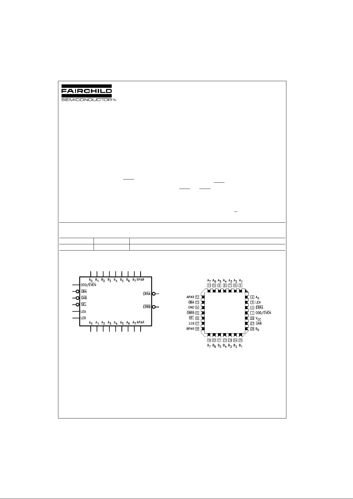
Logic Symbol Connection Diagram
Pin Assignment for PCC
FACT is a tra demark of Fairchild Semico nductor Corporation.
Order Number Package Number Package Description
74ACT899QC V28A 28-Lead Plastic Lead Chip Carrier (PLCC), JEDEC MO-047, 0.450” Square
www.fairchildsemi.com 2
74ACT899
Pin Descriptions Functional Description
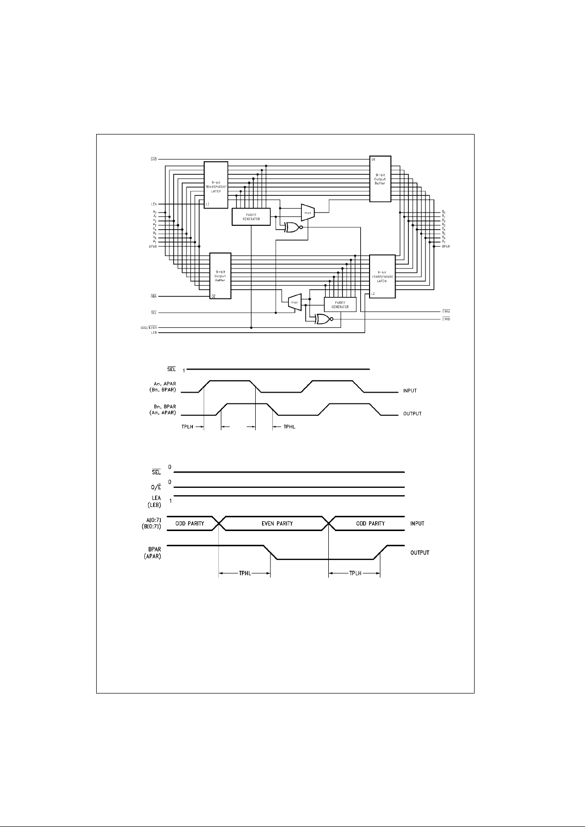
The ACT899 has three prin cipal m odes o f opera tion which
are outlined below. These modes apply t o both the A- to-B
and B-to-A directions.
• Bus A (B) communicates to Bus B ( A), parity is generated and passed on to the B (A) Bus as BPAR (APAR). If
LEB (LEA) is HIGH and t he Mode Sele ct ( SEL
) is LOW,
the parity generated from B[0:7] (A[0:7]) can be checked
and monitored by ERRB
(ERRA).
• Bus A (B) communicates to Bus B (A) in a feed-through
mode if SEL
is HIGH. Parity is still generated and
checked as ERRA
and ERRB in the feed-th rough mo de
(can be used as an interru pt to signal a data/parity bit
error to the CPU).
• Independent Latch E nables (LEA and LEB) allow oth er
permutations of generating/checking (see Function
Table).
Function Table
H = HIGH Voltage Level
L = LOW V oltage Level
X = Immaterial
Note 1: O/E
= ODD/EVEN
Pin Names Description
A
0–A7
A Bus Data Inputs/Data Outputs
B
0–B7
B Bus Data Inputs/Data Outputs
APAR, BPAR A and B Bus Parity Inputs
ODD/EVEN
ODD/EVEN Parity Select,
Active LOW for EVEN Parity
GBA
, GAB Output Enables for A or B Bus,
Active LOW
SEL
Select Pin for Feed-Through or Generate
Mode, LOW for Generate Mode
LEA, LEB Latch Enables for A and B Latches,
HIGH for Transparent Mode
ERRA
, ERRB Error Signals for Checking Generated
Parity with Parity In, LOW if Error Occurs
Inputs Operation
GAB
GBA SEL LEA LEB
H H X X X Busses A and B are 3-STATE.
H L L L H Generates parity from B[0:7] based on O/E
(Note 1). Generated parity → APAR.
Generated parity checked against BPAR and output as ERRB
.
H L L H H Generates parity from B[0:7] based on O/E
. Generated parity → APAR. Generated
parity checked against BPAR and output as ERRB
. Generated parity also fed back
through the A latch for generate/check as ERRA
.
H L L X L Generates parity from B latch data based on O/E
. Generated parity → APAR.
Generated parity checked against latched BPAR and output as ERRB
.
HLHXHBPAR/B[0:7] → APAR/A0:7] Feed-through mode. Generated parity checked
against BPAR and output as ERRB
.
HLHHHBPAR/B[0:7] → APAR/A[0:7]
Feed-through mode. Generated parity checked against BPAR and output as ERRB
.
Generated parity also fed back through the A latch for generate/check as ERRA
.
L H L H L Generates parity for A[0:7] based on O/E
. Generated parity → BPAR. Generated
parity checked against APAR and output as ERRA
.
L H L H H Generates parity from A[0:7] based on O/E
. Generated parity → BPAR. Generated
parity checked against APAR and output as ERRA
. Generated parity also fed back
through the B latch for generate/check as ERRB
.
L H L L X Generates parity from A latch data based on O/E
. Generated parity → BPAR. Gen-
erated parity checked against latched APAR and output as ERRA
.
LHHHLAPAR/A[0:7] → BPAR/B[0:7]
Feed-through mode. Generated parity checked against APAR and output as ERRA
.
LHHHHAPAR/A[0:7] → BPAR/B[0:7]
Feed-through mode. Generated parity checked against APAR and output as ERRA
.
Generated parity also fed back through the B latch for generate/check as ERRB
.
3 www.fairchildsemi.com
74ACT899
Functional Block Diagram
AC Path
An, APAR → Bn, BPAR
(B
n
, BPAR → An, APAR)
FIGURE 1.
An → BPAR
(B
n
→ APAR)
FIGURE 2.
 Loading...