Fairchild Semiconductor 74ABT16373CMTD, 74ABT16373CSSCX, 74ABT16373CSSC, 74ABT16373CMTDX Datasheet

March 1994
Revised November 1999
74ABT16373
16-Bit Transparent D-Type Latch with 3-STATE Outputs
General Description
The ABT16373 contains sixteen non-inverting latches with 3-STATE outputs and is intended for bus oriented applications. The device is byte controlled. The flip-flops appear transparent to the data when the Latch Enable (LE) is HIGH. When LE is LOW, the data that meets the setup time is latched. Data appears on the bus when the Output Enable (OE) is LOW. When OE is HIGH, the outputs are in high Z state.
Features
■Separate control logic for each byte
■16-bit version of the ABT373
■High impedance glitch free bus loading during entire power up and power down cycle
■Non-destructive hot insertion capability
■Guaranteed latch-up protection
Ordering Code:
Order Number |
Package Number |
Package Description |
|
|
|
74ABT16373CSSC |
MS48A |
48-Lead Small Shrink Outline Package (SSOP), JEDEC MO-118, 0.300” Wide |
|
|
|
74ABT16373CMTD |
MTD48 |
48-Lead Thin Shrink Small Outline Package (TSSOP), JEDEC MO-153, 6.1mm Wide |
|
|
|
Devices also available in Tape and Reel. Specify by appending suffix letter “X” to the ordering code.
Logic Symbol |
Connection Diagram |
Pin Descriptions
|
Pin Names |
Description |
|
|
|
|
|
|
|
n |
Output Enable Input (Active LOW) |
|
OE |
||
|
LEn |
Latch Enable Input |
|
|
D0–D15 |
Data Inputs |
|
|
O0–O15 |
Outputs |
|
Outputs STATE-3 with Latch Type-D Transparent Bit-16 74ABT16373
© 1999 Fairchild Semiconductor Corporation |
DS011666 |
www.fairchildsemi.com |

74ABT16373
Functional Description
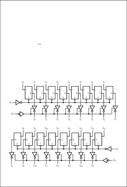
The ABT16373 contains sixteen D-type latches with 3- STATE standard outputs. The device is byte controlled with each byte functioning identically, but independent of the other. Control pins can be shorted together to obtain full 16-bit operation. The following description applies to each byte. When the Latch Enable (LEn) input is HIGH, data on the Dn enters the latches. In this condition the latches are transparent, i.e., a latch output will change states each time its D input changes. When LEn is LOW, the latches store information that was present on the D inputs a setup time preceding the HIGH-to-LOW transition of LEn. The 3- STATE standard outputs are controlled by the Output Enable (OEn) input. When OEn is LOW, the standard out-
puts are in the 2-state mode. When OEn is HIGH, the standard outputs are in the high impedance mode but this does not interfere with entering new data into the latches.
Logic Diagrams
Truth Tables
|
|
|
Inputs |
|
Outputs |
|||
|
|
|
|
|
|
|
|
|
|
|
|
|
|
|
|
|
|
|
LE1 |
|
|
OE1 |
D0–D7 |
O0–O7 |
||
|
X |
|
|
H |
X |
Z |
||
|
H |
|
|
L |
L |
L |
||
|
H |
|
|
L |
H |
H |
||
|
L |
|
|
L |
X |
(Previous) |
||
|
|
|
|
|
|
|
||
|
|
|
|
|
|
|
||
|
|
|
|
Inputs |
|
Outputs |
||
|
|
|
|
|
||||
|
LE2 |
|
|
|
|
|
|
|
|
OE2 |
D8–D15 |
O8–O15 |
|||||
|
X |
|
|
H |
X |
Z |
||
|
H |
|
|
L |
L |
L |
||
|
H |
|
|
L |
H |
H |
||
|
L |
|
|
L |
X |
(Previous) |
||
|
|
|
|
|||||
H = HIGH Voltage Level |
|
|
||||||
L = LOW Voltage Level |
|
|
||||||
X = Immaterial |
|
|
||||||
Z = High Impedance |
|
|
||||||
Previous = |
previous output prior to HIGH-to-LOW transition of LE |
|||||||
www.fairchildsemi.com |
2 |
 Loading...